LED Semiconductor Lighting Network News We have briefly introduced the thermal transient test method of LED junction temperature. This method uses the heat sensitive parameter of the LED itself - voltage change to calculate the temperature rise, so as to get the junction temperature under working condition. So, in addition to the method of testing, is there any other way to know the junction temperature when the device is working? Industry veterans must know that the junction temperature can actually be calculated!
However, before calculating, we must know the thermal resistance of the device (the thermal resistance of the general device specification), and then use the thermocouple to measure the pin temperature or the case temperature to calculate the junction temperature. So what is the thermal resistance? How does the junction temperature calculate using the thermal resistance and the shell temperature? Here are some explanations for everyone.
First, what is thermal resistance?
First of all, in order to make it easier for everyone to understand, we can borrow the concept of electricity. The concept of thermal resistance is derived from the concept of analog resistance. The similarity between the two is very high. Resistance refers to the physical quantity that hinders current conduction. Correspondingly, thermal resistance is the physical quantity that hinders heat flow conduction. Under the same conditions, the greater the thermal resistance, the less easily the heat flow passes.
If a heat source is connected to several heat conduction paths with unequal thermal resistance values, the heat flow size distribution is the same as the current when the current flows through different resistors, as shown in Figure 1.
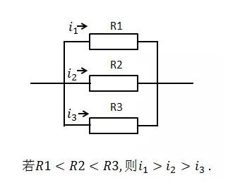
Current (heat flow) profile
That is to say, if there are several heat conduction paths between two isothermal points, one of which has a very large thermal resistance value and the other has a very small thermal resistance value, the heat is almost always from the thermal resistance value. The small path passes, which is the theoretical basis that will be quoted below.
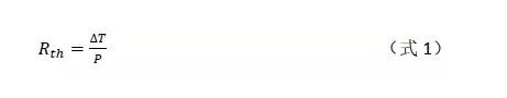
Next, let's look at the physical definition of thermal resistance. The so-called definition is to tell us how to calculate the thermal resistance value. As mentioned above, the definition of thermal resistance can be analogized to resistance. The resistance is the ratio of the voltage difference ΔU across the conductor to the current I through the conductor. Then we can easily understand the definition of thermal resistance. The thermal resistance is defined as the ratio of the temperature difference ΔT across the material on the heat flow path to the thermal power P flowing through the channel. Formula expression is
After warming up, please go into the JESD51-1 standard to see the thermal resistance of the semiconductor device.
1.1 Thermal resistance structure
The thermal resistance of semiconductor devices is defined in detail in the JESD51-1 standard.
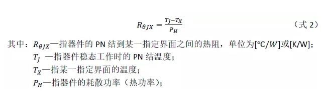
We can see that (Equation 2) is actually a complementary form of (Equation 1), and it is quite intuitive and convenient to analyze the structure of a semiconductor device such as an LED by (Equation 2).

LED package structure sectional view
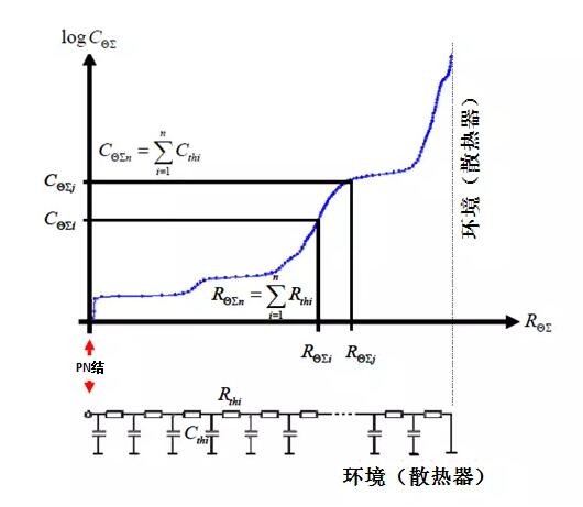
Taking the package structure of the common LED in Fig. 2 as an example, it is assumed that the heat generated by the heat source is conducted from the PN junction all the way down, passing through the chip-solid crystal layer-device holder-thermal paste-heat sink, and the heat sink and the ambient temperature are considered to be thermally balanced. So how do you know the exact thermal resistance of the PN junction to the bottom of the device holder? Let us introduce a new analysis method - structure function method.
1.2 structure function
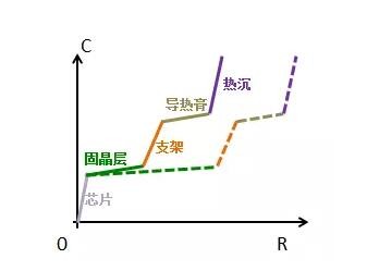
We refer to a function that can describe the thermal resistance heat capacity structure of the material inside the semiconductor device as a structure function. In the structure function, the thermal resistance heat capacity characteristics of each material can be expressed intuitively, as shown in Figure 3. As the ladder, from left to right, the chip, the solid crystal layer, the support, the thermal paste, the heat sink .

Device structure and structure function
Mentioned here, by the way, readers will review again. In the previous article, we mentioned that whether it is a diode, a triode, a FET or an IGBT, the junction temperature and thermal resistance of these semiconductor devices can be measured by T3ster. Moreover, after the mathematical operation, the thermal resistance of each layer structure on the heat conduction path can be analyzed to find the heat dissipation bottleneck. What is said here is actually the power of the structure function. If there is a problem with the material of one of the layers inside the device (such as the solid crystal layer), it can be clearly expressed in the structure function function, as shown in Figure 4.
The difference between the solid crystal anomaly in the structure function (the solid line is the solid crystal normal sample, and the broken line is the solid crystal abnormal sample)
The abnormality of the solid crystal is manifested by the increase of the thermal resistance of the solid crystal layer, so that the structure under the solid crystal is translated to the right side of the normal sample curve. Through the structure function, we don't need to destroy the sample to give out the abnormalities that are invisible to the inside of the device, just like X-ray! With the structure function, whether you want to know which interface to which interface thermal resistance, we can divide it layer by layer, the aforementioned mentioned the thermal resistance value of the PN junction to the bottom of the device holder is Nothing to say.
Well, we get the thermal resistance (called) from the PN junction we want to know to the bottom of the device holder through the structure function. The thermal resistance of the device given in the specifications of the general device is strictly this. Now let's answer the question mentioned at the beginning of the text: How to use this thermal resistance value to calculate the junction temperature.
Second, the use of thermal resistance to calculate junction temperature
Representing the thermal resistance of the PN junction to the bottom of the bracket, we can use (Formula 2) and shift the term (Formula 2) to get
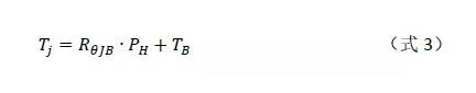
Which refers to the temperature at the bottom of the bracket. Generally, we can't measure the temperature at the bottom of the bracket, because the bottom of the bracket has been soldered to the aluminum substrate or the common FR4 substrate. Although we can't get the value, we can approximate the method. In fact, the most commonly used test method is to use the thermocouple to test the temperature of the contact point between the bracket shell and the substrate when the device is working, as shown in Figure 5 and Figure 6. We generally refer to this temperature. In other words, we are taking it.
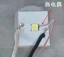
Test the outer edge temperature of the lamp holder with a thermocouple
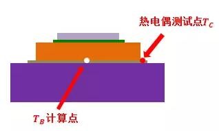
Position map
There will be a certain temperature difference between the two points and, in general, it is. After the approximation, (Equation 3) becomes

. To use (Equation 4), we must also know the thermal power of the device, which can be passed.
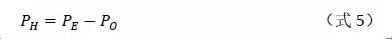
Seek.
This refers to electrical power and refers to optical power. For LED devices, the thermal power can only be obtained by subtracting the optical power from the electric power, and the optical power can be measured by the integrating sphere. For a semiconductor device that does not emit light, its thermal power is directly equivalent to the electric power, which can be directly substituted into the calculation. . In this way, we can calculate the junction temperature by measuring the thermal resistance of the device on the specification and the thermocouple to measure the pin temperature or case temperature.
Maybe everyone will be wondering, how did this amazing structure function come out?
You should remember that we have mentioned the transient test method of "current jump". If we continuously collect the voltage signal after the jump, until the device cools to the ambient temperature, we can get the LED during the cooling process. Its voltage vs. time curve, and because these voltage changes are obtained under the test current, we only need to divide the voltage signal by the K factor to get the temperature change curve with time (because), the temperature change curve Figure 1 shows:

Temperature change-time curve
Time logarithmization
In fact, the timeline in Figure 1 is logarithmic, because we actually benefit from the high-speed sampling of the device at 1? ? After s (ie s), the change value of the first voltage is collected, but the order of the total sampling time is generally in the range of 1 s to s. The magnitude of the time span is large and the temperature changes more slowly after the time, the data is important. The degree is also reduced, so we log the time in the data processing. The time-logged curve is shown in Figure 2b.
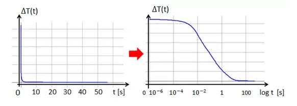
Figure 2a Temperature change response curve Figure 2b Temperature change response curve (after time logarithm)
Comparing Fig. 2a with Fig. 2b, it can be found that the data change before the logarithmic preprocessing is not intuitive, and the logarithmic processing can fully express the temperature change within a few microseconds after the transient switching. The derivation of time logarithm is also used in the calculation.

This time we use this curve to get our magic structure function. First of all, we must introduce:
Physical model of the RC network
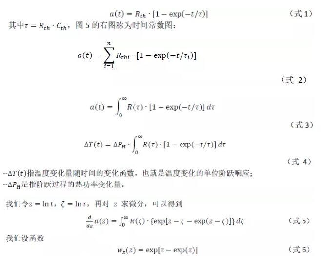
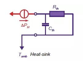
First, we need to construct a thermally conductive model. It is better to start with simplicity, assuming that there is only one path for heat conduction from the heat source to the environment, and it is a material that is isotropic and regular in shape, has a certain thermal resistance and heat capacity, and we also use resistors and capacitors. The symbol is used to represent the thermal resistance and heat capacity, and the heat source flows from the left surface of the material to the right surface (environment), as shown in Figure 3.
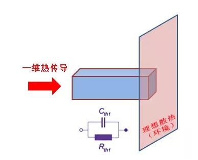
Heat conduction model diagram and RC network
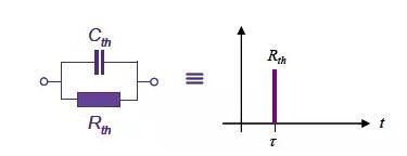
In this simple model, we see an RC (resistance-capacitor) network, as shown in Figure 4. In this network, the heat source acts as a constant current source, and the thermal resistance and heat capacity are connected in parallel to the environment. It is a first-order RC network.
First-order RC network
In the field of digital signal processing, the response of a system is usually used to analyze the structure of the system. The so-called response is the reaction (output characteristic) generated by the system under the excitation of a specific signal source. For example, someone shouts your name behind you, some people will look back and others will not look back. Different systems will have different responses, and the same system will respond differently under different signal excitations.
Now that we consider this first-order RC network as a system, what signal should we use to motivate it? In fact, the "current jump" we mentioned at the beginning of the text can be used as a signal source. Generally, we call this current jump signal a unit step signal because its signal suddenly jumps from low to high like a step. (or from high to low), what is the response of this system under unit step signal excitation?
If the input signal is a unit step signal, the response of this system is simply referred to as the unit step response of the system.
Then the unit step response of the first-order RC network is (Equation 1)
The right graph of Figure 5 is called the time constant graph:
First-order RC network and corresponding time constant graph
In Equation 1, we call the time constant, which is a commonly used physical quantity that characterizes time in the field of signal processing. Its dimension unit is the same as time, and it is also seconds [s]. The meaning of the time constant refers to the time required for a physical quantity to decay from the maximum value to 1/e of the maximum value (or increase from the minimum value to 1-1/e times the maximum value). For example, a fully charged capacitor is connected in parallel at both ends. A resistor, then the time it takes for the voltage across the capacitor to discharge from the maximum value to 1/e times the maximum value.
Here we call the "thermal time constant" to distinguish it because it represents the product of thermal resistance and heat capacity.
Now that we have upgraded the number of structures from one to n, we will become an n-order RC network, as shown in Figure 6.
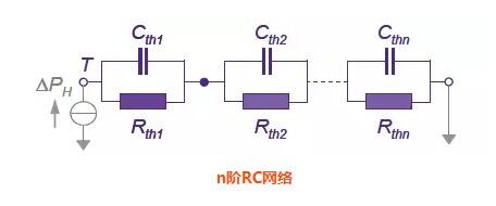
N-order RC network
The corresponding unit step response is (Equation 2)
Generally, we refer to the RC network of this structure as an n-order Foster structure, and its corresponding thermal time constant spectrum is shown in Fig. 7.
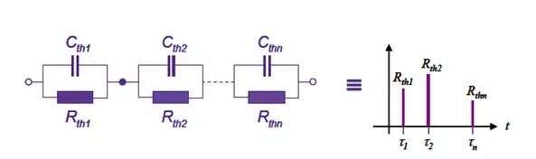
Thermal time constant diagram of n-order Foster structure
In fact, the interface between the material and the material has the same thermal resistance and heat capacity. It is impossible for the materials of the device to be completely independent of a single thermal resistance. We should consider the thermal resistance and the heat capacity. The change is continuous, so we need to continue this discrete polynomial, that is, when n tends to be positive infinity, we can change (Formula 2) to (Formula 3).
In the equation (3), called the time constant spectral function, we replace the discrete ones with continuous ones. Its time constant graph is a continuum, as shown in Figure 8.
Continuous spectrum
(Formula 3) This formula represents the unit step response of a continuous RC network.
Look at the temperature change curve of Figure 1b at the beginning of the text. In fact, the corresponding expression of this curve before the logarithm processing is (Formula 4).
- refers to the function of the change in temperature over time, that is, the unit step response of temperature changes;
-- refers to the amount of thermal power change in the step process.
Solving the thermal time constant spectral function
Let's look back. In fact, if we know the expression, then we are equivalent to knowing the relationship between the thermal resistance and the heat capacity of the system, that is, knowing all the structures of this system (Foster Network). So in order to get the thermal resistance heat capacity structure of our system, the following will start to find out:
We can further differentiate, we can get (Equation 5), we set the function (Equation 6), then (Equation 5) can be expressed as (Formula 7) to observe the form on the right, which is actually the most common convolutional form in signal processing, ie ( Equation 8) represents the convolutional symbol, and Equation 8 and Equation 7 are completely equivalent, except that the arithmetic symbols are different.
Then, the expression that can be found is: (Equation 9)
The deconvolution symbol is the inverse of the convolution (such as division by multiplication).
Here we get the analytical form, one step away from the structure!
Let us look at (Equation 9), which is a known integrable function, which is the differential of the unit step response (after time logarithm), that is, the derivative, which we can all calculate by computer. The only thing left is the deconvolution operation. There are many methods for deconvolution operations, such as Bayesian deconvolution method and Fourier frequency domain deconvolution method, which are very mature algorithms. There is more knowledge involved here, and they will not be developed one by one.
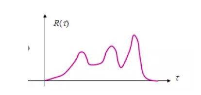
Now we get the thermal time constant spectrum function, the actual image is shown in Figure 9.

Thermal time constant spectrum of the actual sample
This function image is obtained through the above mathematical transformation and mathematical operation. We will use this function to analyze the thermal resistance heat capacity structure.
From the figure, we can clearly see that the different amplitudes have different fluctuations and exhibit a certain degree of dispersion. We define the thermal time constant spectrum function from this: (Equation 10)
Simply put, this function is cut into a number of small pieces, and these small pieces are spliced ​​together. And each of these small blocks corresponds to the first-order Foster structure, as shown in Figure 10.
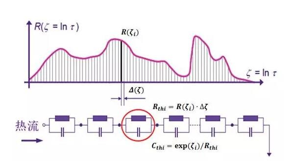
Correspondence between thermal time constant spectral function image and nth-order Foster network
According to the definition, we can get (Equation 11) and then, and get (Equation 12)
In this way, we calculate the thermal resistance and heat capacity in the thermal resistance heat capacity structure by Equations 11 and 12.
Foster-Cauer Network Conversion
Many readers should think that this is over, but in fact, this is only the thermal resistance of the Foster network.
The heat capacity in the Foster network model is the node-to-node heat capacity value, which is inconsistent with the actual situation of the device, and has no corresponding physical meaning. why? Here we leave this small problem to everyone (hint: use capacitors for example, if a system consists of several capacitors in series, how is the relationship between the total capacitance of the system and the individual capacitors?). Therefore, the Foster structure is not suitable for describing the thermal resistance heat capacity characteristics of our semiconductor devices.
Although the Foster structure is not suitable for describing the actual device, there is another structure that can be converted to it. This structure is called the Cauer structure, as shown in Figure 11.
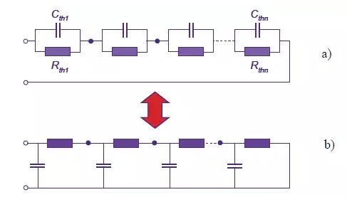
a) Foster structure; b) Kaul structure
The Foster structure and the Caul structure are equivalent for single-ended passive RC networks because they can be converted to each other, but the Kaul structure is exactly the same as the thermal resistance heat capacity structure of the device we are talking about. The reason why so many Foster structures are discussed is that its time constant calculation is a very good mathematical method, while reducing many complicated calculations.
Due to the limited space, the conversion process of these two networks will not be described here. After the conversion, we will get a new expression of the sum.
Drawing structure function
We obtained the thermal resistance and heat capacity of the Coral network, but these parameters can not be visually represented. We now use the model constructed in Figure 3 to represent this resistance structure, as shown in Figure 12.
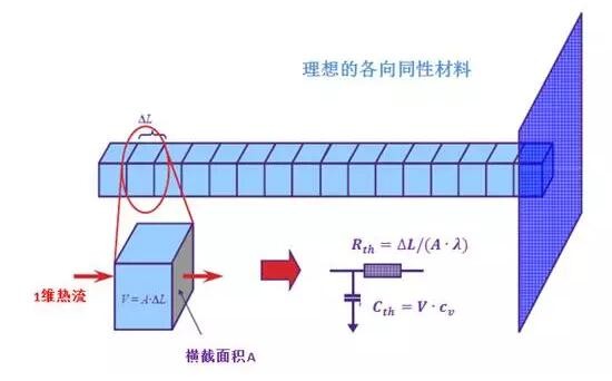
Ideal one-dimensional heat conduction model
In Fig. 12: represents the thickness of the material parallel to the heat flow path; A represents the cross-sectional area of ​​the material perpendicular to the heat flow path; represents the thermal conductivity of the material; represents the heat capacity value per unit volume. We can derive the expression of total thermal resistance and total heat capacity:
(Equation 13) and (Equation 14)
Using (Equation 13) and (Equation 14), combined with the thermal resistance and heat capacity corresponding to the Kaul network, we get the structural function we are struggling to pursue, as shown in Figure 13:
Correspondence between Kaul structure and structure function
At this point, our derivation of the structure function is finally over~
In the end, we will show the whole derivation in the form of a flow chart, as shown in Figure 14:
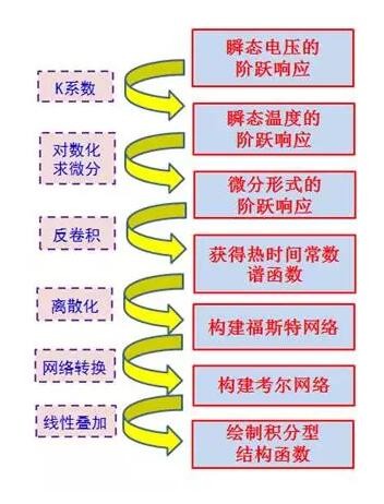
Structure function derivation flow chart
This article is provided by the LED- FPD Engineering Technology Research and Development Center of Hong Kong University of Science and Technology, Foshan.
Oubaibo has been committed to the development and manufacture of high-quality slip rings for many years. We are a well-known professional manufacturer of slip rings, such as through bore slip ring, slip ring connector, Ethernet Slip Ring, Conductive Slip Ring, fiber slip ring, etc. Please feel free to contact us for more details.
Custom Slip Ring,Rotary Joint Price,High Pressure Rotary Joint,Moflon Rotary Union
Dongguan Oubaibo Technology Co., Ltd. , https://www.sliprob.com