With the continuous innovation and rapid development of the lighting industry, coupled with the increasing importance of energy saving and environmental protection, high-brightness (HB) LEDs have evolved from simple indicator lights to important lighting sources that go beyond traditional light sources. Compared to other lighting solutions, HB LEDs offer several significant advantages such as low power consumption, long life and high quality lighting. However, in order for HB LEDs to successfully replace ordinary incandescent lamps into high-volume markets, the cost of driving electronic devices must be minimized.
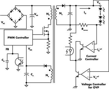
Figure 1 Traditional secondary side regulated offline LED driver
For traditional lighting incandescent lamps, driving is a breeze, just connect the bulb directly to the voltage source. Most energy sources are in the form of a constant voltage, which makes the driving cost of incandescent lamps quite low. However, LEDs have a light output intensity that is proportional to its current and forward voltage drop and varies with temperature. Therefore, the LED requires a constant current to drive and requires additional circuitry. Traditionally, off-line constant current drivers for LEDs have typically been implemented using isolated flyback converters with output current regulation circuitry (see Figure 1). The actual LED voltage is measured by a sense resistor and then compared to the reference voltage value to obtain the error voltage. The error voltage is transmitted to the primary side via an optocoupler for controlling the duty cycle of the primary side switching device. Although this solution enables excellent LED current regulation, the output regulation circuit requires an optocoupler, a reference voltage, and a sense resistor, which greatly increases system cost and reduces overall efficiency.
Primary side regulation (PSR) technology may be the best solution to minimize the cost of off-line LED drivers. This technology requires only the information on the primary side of the driver to accurately control the LED current at the secondary side, eliminating the output current sense loss and eliminating all secondary feedback circuitry, thereby improving the offline LED driver without incurring significant cost. The efficiency of the design. In addition, the technology can adjust the LED driver output voltage without the need for a secondary-side feedback circuit, which is equivalent to providing an over-voltage over-voltage protection function to further ensure the reliability of the driver. This article will discuss the basic working principle of the primary-side regulation technique and introduce a highly integrated primary-side regulation PWM controller. This controller has several significant advantages over traditional secondary end regulation methods.
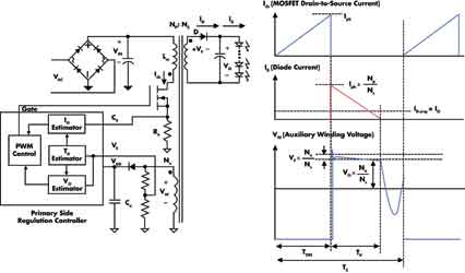
Figure 2 Primary-side regulated offline LED driver and its typical waveform
Basic concept of primary end regulation
Figure 2 is a basic circuit diagram of a primary-side regulated flyback converter and its typical waveform. In general, the discontinuous conduction mode (DCM) output regulation performance is better, so it is the preferred mode of operation for primary-side regulation. The key to primary side regulation is how to obtain output voltage and current information without direct detection. Once these values ​​are obtained, they can be easily controlled by traditional PI control methods.
The primary side inductor (Lm) is loaded with the input voltage (VIN) during the MOSFET on-time (TON). Thus, the MOSFET current (Ids) increases linearly from 0 to the peak (Ipk). During this time, energy is transferred from the input to the inductor. When the MOSFET is turned off, the energy stored in the inductor causes the rectifier diode (D) to conduct. During the diode on-time (TD), the output voltage (Vo) is applied to the secondary side inductor (Lm × Ns2 / Np2), and the diode current (ID) linearly drops from the peak (Ipk × Np / Ns) to zero. At the end of the TD, all of the energy stored in the inductor is released to the output. During this time, the sum of the output voltage and the forward voltage drop of the diode is reflected to the auxiliary winding end, expressed as (Vo + VF) × Na / Ns. Since the forward voltage drop of the diode decreases as the current decreases, the diode current decreases to zero at the end of the diode conduction time, so that the auxiliary winding voltage best reflects the output voltage. Therefore, by simply sampling the winding voltage at the end of the diode conduction time, the output voltage information can be obtained, and the diode conduction time can be obtained by monitoring the auxiliary winding voltage.
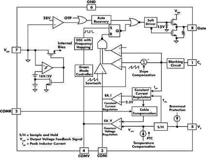
Figure 3 Schematic diagram of the internal module of the integrated power switch (FSCQ-series)
At the same time, the estimation of the output current requires some multiplication calculations. Assuming that the output current is equal to the average current of the diode at steady state, the output current can be estimated by the following equation: Io = Ipk × (Np / Ns) × (TD / 2Ts). The output current estimator obtains the peak value of the drain current through a peak detection circuit and calculates the output current using the diode conduction time (TD).
Integrated primary side regulation controller
The primary-side regulated PWM controller, such as Fairchild Semiconductor's FAN102, is a technology that specializes in the design of primary-side regulated offline LED drivers. This technology significantly simplifies design challenges for more demanding efficiency and eliminates the need for external components that add cost and reliability issues, such as optocouplers and the KA431. FIG. 3 is a schematic diagram of an internal module of the FAN 102. The device features an internal reference voltage with ±1% tolerance for the error amplifier, minimizes input current/voltage variations based on tolerances from external components, and an integrated external component temperature variation compensation circuit. High precision can be obtained regardless of the temperature change. Its internal oscillator has a frequency hopping function to reduce EMI, and a small line filter can be used at the input.
in conclusion
The proprietary technology that combines sampling and output estimation provides an accurate, lower-cost implementation for a variety of off-line LED drivers—from streetlights to medical applications to consumer electronics applications such as cabinet lights and desk lamps. These LED drivers are now able to achieve smaller size, lower cost and higher efficiency.
Editor: China Lighting Network - Wheat
Bluetooth speaker is a kind of speaker unit which is used for multimedia devices. They have loud sound, wide frequency response range and rich bass.
Our main Multimedia Speakers are full ranges speakers units:
1) From the diameter: we have speakers in 1" ~ 3".
2) From the power output, we have speakers of 2W ~ 15W.


FAQ
Q1. What is the MOQ?
XDEC: 2000pcs for one model.
Q2. What is the delivery lead time?
XDEC: 20 days for normal orders, 15 days for urgent orders.
Q3. What are the payment methods?
XDEC: T/T, PayPal, Western Union, Money Gram.
Q4. Can you offer samples for testing?
XDEC: Yes, we offer free samples.
Q5. How soon can you send samples?
XDEC: We can send samples in 3-5 days.
Bluetooth Speaker
Portable Bluetooth Speaker,Mini Bluetooth Speaker,Waterproof Bluetooth Speaker,Lamp Bluetooth Speaker
Shenzhen Xuanda Electronics Co., Ltd , http://www.xdecspeaker.com