In the process of working on an integrated circuit chip, power loss is inevitable, and most of these power losses will be converted into heat energy. In the case of abnormal conditions such as high environment and short circuit, the heat inside the chip cannot be dissipated in time, which inevitably increases the operating temperature of the chip. Excessive operating temperatures have a large impact on chip performance, reliability and safety. Studies have shown that for every 1 °C increase in chip temperature, the drive capability of the MOS transistor will drop by about 4%, the connection delay will increase by 5%, and the integrated circuit failure rate will double. Therefore, the chip must have an over-temperature protection circuit to protect it. Chip security.
An over-temperature protection circuit that can be implemented in a standard CMOS process will be described. In the circuit design, a current source (PTAT current) proportional to temperature and a PNP tube (parasitic CMOS process) junction voltage with a negative temperature coefficient are used as two differential temperature sensing units. This differential sensing method can improve the sensitivity of the circuit to the temperature change reaction, and at the same time, it has a hysteresis function, which can effectively avoid damage to the chip caused by thermal oscillation.
This article refers to the address: http://
1 Architecture principle analysis
1.1 Working principle analysis Figure 1 is the principle architecture of the design. Q1 is a parasitic PNP transistor in the NWELLCMOS process. The collector must be connected to the location. In order to utilize the parasitic PN junction to conduct the negative temperature characteristic of the forward conduction voltage, Connect Q1 as a diode (the base set is also connected to ground), so that the voltage VA between point A and ground has the property of the forward voltage of the PN junction being inversely proportional to temperature. Since the bias voltage of the reference circuit output is applied to the gates of M0, M1, and M5, the PTAT current (Proportional to Abso-lute Temperature) is generated on the branch; when the bias is provided, it is also on the resistor R0. A voltage VB proportional to the temperature is generated, that is, the voltage at point B increases. When a certain temperature TH (set shutdown temperature) is reached, VH ≥ VA, comparator Comp outputs a high level, after the inverter INV, the output TSD is low; this signal acts on other modules of the circuit After that, the entire chip is stopped and the thermal protection function is realized. At the same time, the positive feedback of the TSD signal acts on the M2 gate, turning on M2, increasing the current on the resistor R0, making VB higher.
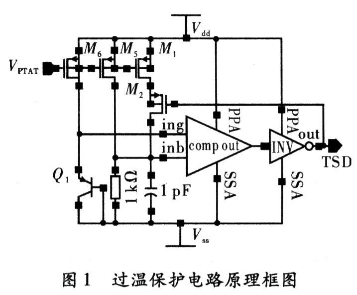
After the chip is thermally protected and stops working, the temperature on the chip will drop from TH, causing the voltage VA at point A to rise slowly, and the voltage VB at point B to slowly decrease. Since the positive feedback action of the previous TSD has caused VB to rise, in this state, the occurrence of VA ≥ VB causes the comparator output to flip. It is necessary that point A has a voltage greater than the previous voltage VA, correspondingly causing the drop. The recovery temperature TL corresponding to the flip point will also be lower than TH. When the temperature is lower than TL, VB ≥ VA, after the action of the comparator, the TSD will output a high level, and the chip will resume operation. At the same time, the TSD signal will still be positively applied to the M2 gate again, turning off M2, further reducing the current on the resistor R0, making VB lower.
During the entire work process, the positive feedback of TSD played a role in hysteresis. In normal operation, the TSD output high level acts on other modules of the circuit. When the temperature is too high, the TSD output low level acts on other modules of the circuit to stop the chip and protect the chip.
1.2 Calculation of temperature rollover point The voltage VA of point A is the voltage on both sides of the PN junction. The expression of the PN junction voltage can be written as 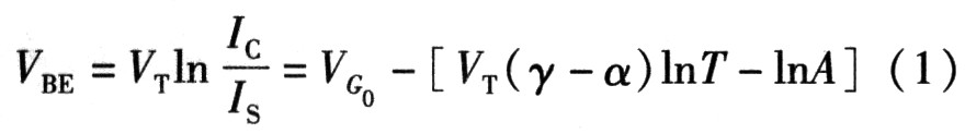
Where VG is the bandgap voltage, γ and α are device parameters, and A represents the temperature-independent constants of those equations pushed into the process. Since Vt = kt / q, it can be seen that VBE decreases with increasing temperature. Its equation about temperature change is 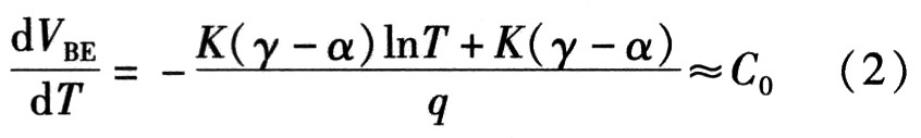
If the influence of the lnT term change on the equation (2) caused by the temperature change is ignored, dVBE/dT can be approximately equal to the constant C0. C0 is about -2 mV/K at normal temperature. In order to simplify the calculation, the equation of variation of the PN junction with respect to temperature can be approximately linear 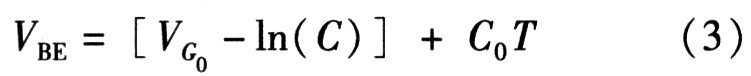
The voltage at point B is the voltage across the resistor and can be calculated from the ohm theorem. The temperature rise flip point TH is calculated. When the temperature rises, it can be seen from the previous analysis that TSD is at a high level and M2 is turned off. Therefore, the current flowing into R0 is only I1. The expression of the VB voltage in this state is 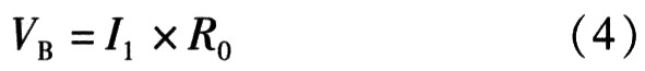
The corresponding equation when flipping the point (VA=VB) is 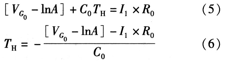
Calculating the temperature drop Flip point TL When falling from above the TH temperature, the pre-analysis shows that TSD is low and M2 is on. Therefore, the current flowing into the resistor R has two paths I1 and I2. The expression of the VB voltage in this state is 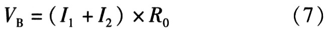
When the rollover point (VA=VB) is used, the corresponding equation is
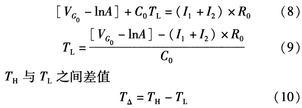
Equation (10) is the amount of hysteresis during overtemperature protection operation.
2 actual circuit design The designed overheat protection circuit is roughly divided into three parts, as shown in Figure 3.
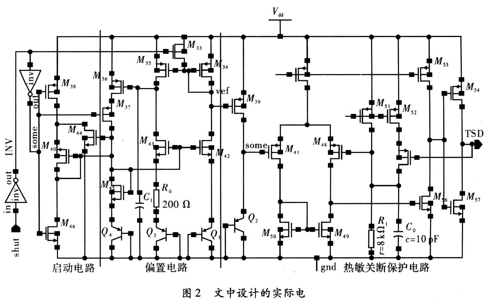
Start circuit: The start circuit will only work when it is just powered on. When the power supply voltage rises slowly from 0 V, and the input signal Shut is low, the switch M37 will be turned on, and the MOS transistor M38 will also be turned on. Pass, this will make the voltage on the branch of M38 slowly rise. The gate terminal of the M40 connected in the form of a diode also rises, and the gate voltage is supplied to the M45, M43, and M42 at the right end, thereby breaking the balance of the reference circuit and enabling it to be activated. When the gate voltage of M40 rises to the threshold voltage of M44, it will be turned on, resulting in a path from the power supply to the ground, thus completing the function of the startup circuit.
The biasing circuit: The working principle of this part of the circuit is basically the same as the principle of generating the PTAT current circuit, and the voltage at the output terminal provides bias for other circuits. The branch consisting of M36, M45 and Q4 will take out the current at the right end branch, after filtering, amplifying and then mirroring back, and outputting a bias voltage signal on the branches of M34, M42 and Q1. Due to the working principle of the current mirror, it is required that M34~M36 and M42~M45 are the same pair of tubes. In addition, in this circuit, M33 is used as the shutdown tube. When the Shut signal is high, M33 will be in the on state, so that M34 and M35 will be turned off this time, so that the whole circuit is turned off.
Thermal shutdown protection circuit: Since the bias voltage of the reference circuit output is applied to the gates of M39, M51, and M52, PTAT current is generated on both branches. The two-stage comparator composed of M41, M47, M48, M49, and M50 is used to realize the function of Comp in the principle equivalent diagram. The first stage of this comparator is the PMOS differential input.
The role of PMOS as a differential input: (1) reduces the input noise. Under normal circumstances, the temperature cannot be changed drastically, so the frequency of temperature fluctuations cannot be very high, so the flicker noise 1/f will become the main component of noise. The PMOS input reduces the effect of noise on the circuit; (2) the PMOS input reduces the lower limit of the common-mode input range. This circuit comparator compares the voltage close to the PN junction VBE, and the input terminal made of PMOS can better meet the requirements of this low common mode input voltage. The second stage of the comparator is a common source amplifier. As the second stage of the comparator, its main function increases the output swing, improves the gain and input resolution, and speeds up the conversion rate of high and low levels. The function of the capacitor C0 in the circuit: the capacitor C0 can suppress the voltage fluctuation generated by the interference amount on the resistance wind of the comparator to the input terminal to prevent the malfunction caused by the disturbance of the system.
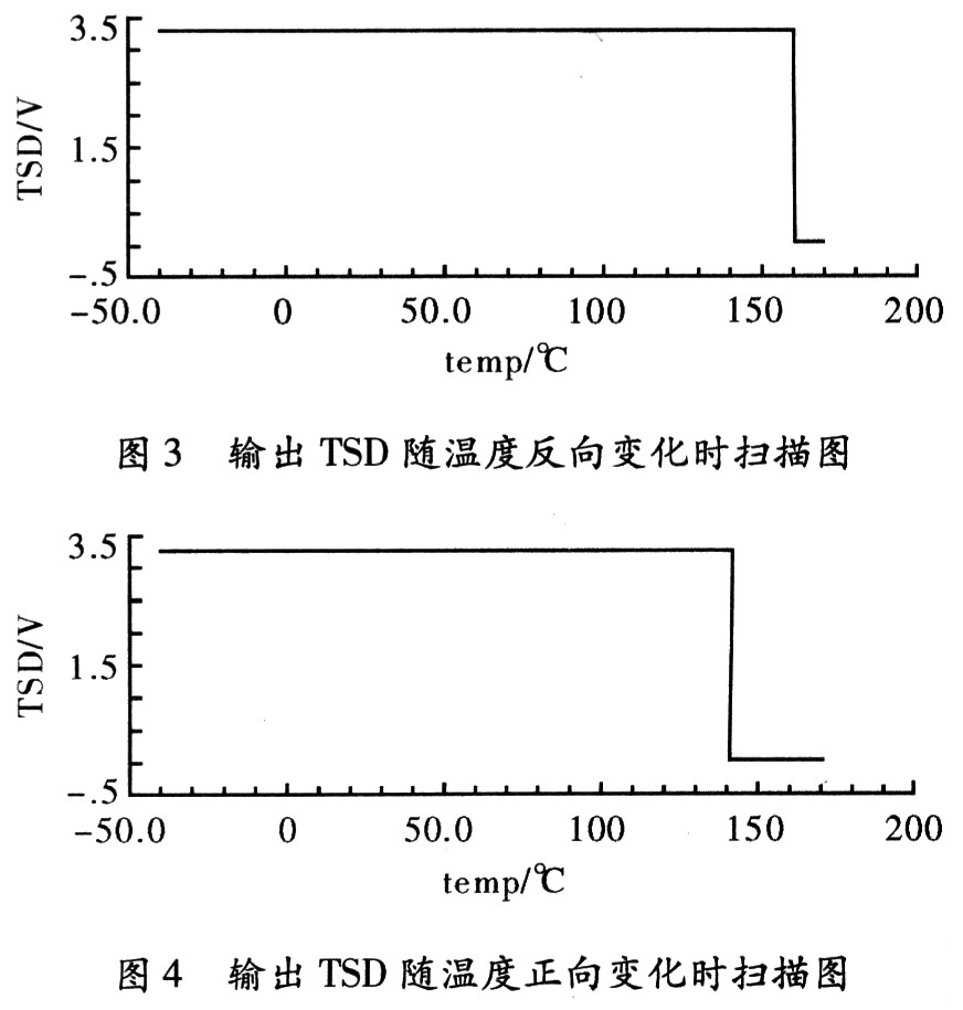
3 Simulation test Follow the circuit designed above. It was simulated with Cadence Specture and the model parameters of the device were in a 0.35 μm CMOS process. Figure 2 is a graph showing the output control signal TSD of the overtemperature protection circuit as a function of temperature rise and fall. The power supply voltage is 3.3 V. It can be seen from the simulation results that the circuit achieves a good "temperature hysteresis" characteristic. The hysteresis function effectively avoids the thermal oscillation of the chip. The shutdown temperature is TH160° and the recovery temperature is TL140°.
4 Conclusion The overheat protection circuit designed in this paper uses PTAT current to detect the temperature change and convert it into a voltage signal input two-stage comparator for comparison, thus generating an overheat protection signal. The hysteresis effect of the comparator can effectively prevent the occurrence of thermal oscillations. The circuit is sensitive to temperature sensing and is ideal for integration in integrated circuit chips.
Privacy Screen Protector:
Privacy Screen Protector looks and feels amazing. It is mostly used for mobile phones, tablets and laptops. Screen is only visible to persons directly in front of screen and other people on both sides only see darkness. Privacy Tempered Glass can effectively protect your privacy and sensitive information from prying eyes.
Pls feel free to contact us if you are interested in these products, have any questions or special needed. We have the best sales team to service to you.
Look forward to your inquiry, and welcome to visit our factory.
Privacy Screen Protector
Privacy Screen Protector,Privacy Glass Screen Protector,Privacy Tempered Glass,Privacy Glass Protector,Iphone Glass Protector
Shenzhen Kantou IM Technology Co., Ltd. , http://www.kantou-im.com