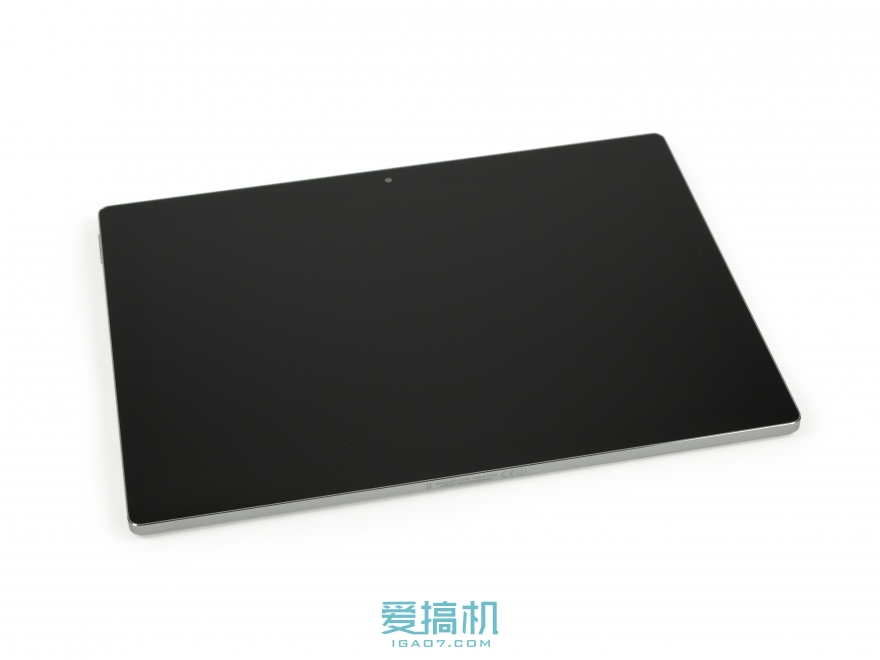
The well-known foreign disassemble team has recently adopted the Google Pixel C Tablet PC equipped with the Terga X1 SoC. The design style of the aircraft is similar to that of the Microsoft Surface Pro/Apple iPad Pro. It adopts the design concept of the tablet + combination keyboard. After being unabashed in the new-style PC era, Google joined the ranks of "2 in 1" following Microsoft and Apple. Pixel C uses a 20.6 x 1800 resolution 10.2-inch LTPS LCD screen with a PPI of 308 and a maximum screen brightness of 500 nits. The aircraft is equipped with a Tegra X1 SoC called the second generation of nuclear bombs. The chip uses a 20-nanometer process and has a maximum frequency of 1.9 GHz. The CPU uses a 4×A57+4×A53 combination. Today we will take a look at the internal design of Pixel C.
10.2 inch LTPS screen with 2560 X 1800 resolution (308 PPI)
NVIDIA Tegra X1 64-bit Quad-Core Processor with 256 Maxwell Core GPU Processors
3 GB LPDDR4 running memory
32 or 64 GB of built-in storage
USB Type-C interface
8MP rear camera + 2MP front camera
Equipped with Android 6.0 Marshmallow marshmallow system
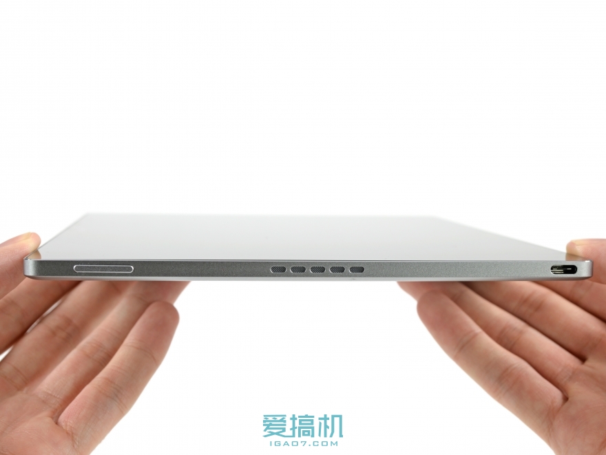
The Pixel C features an aluminum monolithic body with stereo speakers, USB Type-C connectors, and volume buttons on the bottom.

The power button is located at the top of the main body, and there are four noise-canceling microphones in the middle. However, the machine does not support the use of "OK, Google" to wake up.

The display panel and the body are glued and fixed, so the screen needs to be heated first.
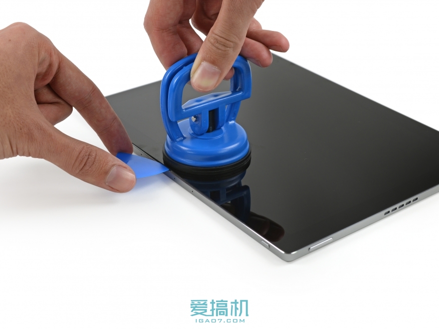
After heating, use a suction cup and paddle to slowly lift the screen along the edge of the screen.

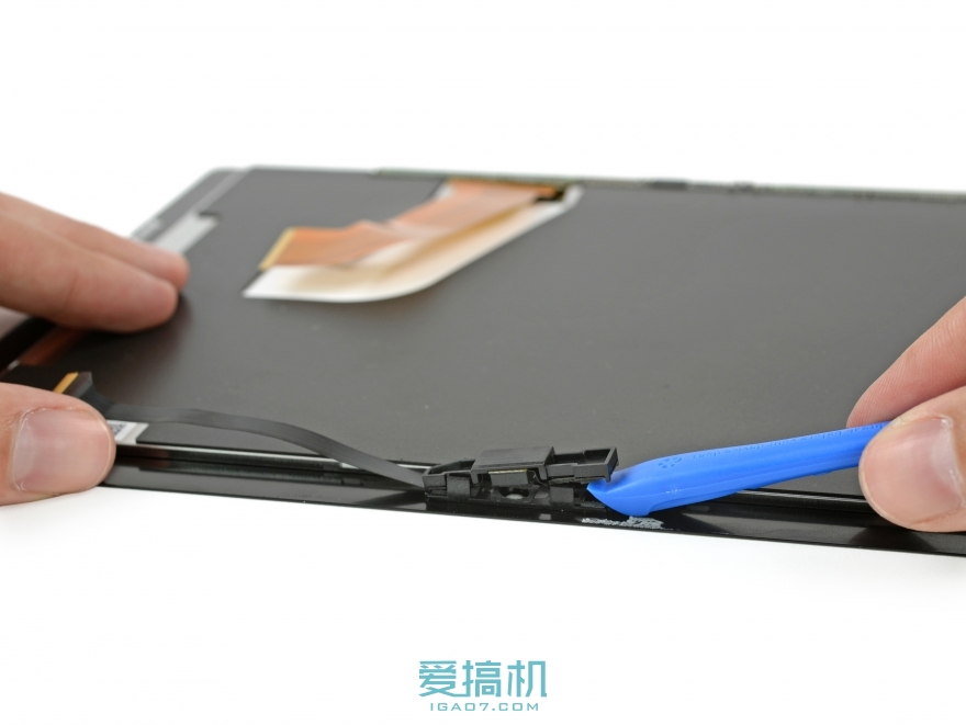
Slowly detach the adhesive at the bottom of the entire screen along the screen. It should be noted that the camera is connected to the mainboard through the cable, and the cable needs to be dismantled before further dismantling.

You can then turn on the entire screen. Note that there is a very wide line at the bottom of the screen. Take care when removing it.
After removing the screen, we first remove the front camera. Unlike most mobile phones and flat-panel designs, the front camera is snap-fitted onto the display panel.

The front camera is 2 million pixels, and there is a front ambient light sensor and LED indicator next to the camera.

The lower part of the display has a small circuit board that controls display and touch.
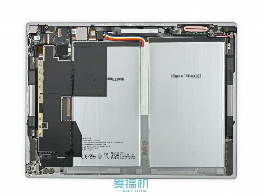
The first part of the fuselage is greeted by a large, built-in battery. To ensure that the circuit is not damaged during the dismantling process, we first remove the battery cable.
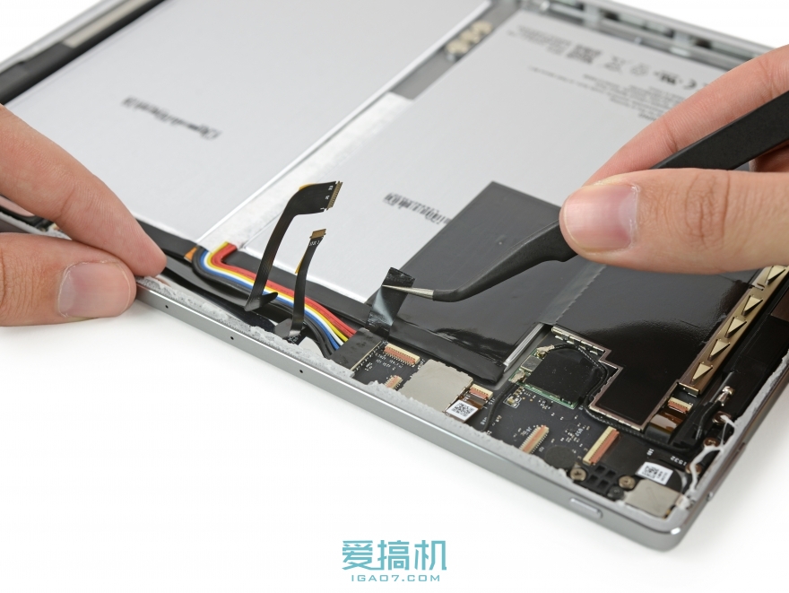
The battery cables are concealed under the two black cables and tape, and they need to be removed before they can be removed.
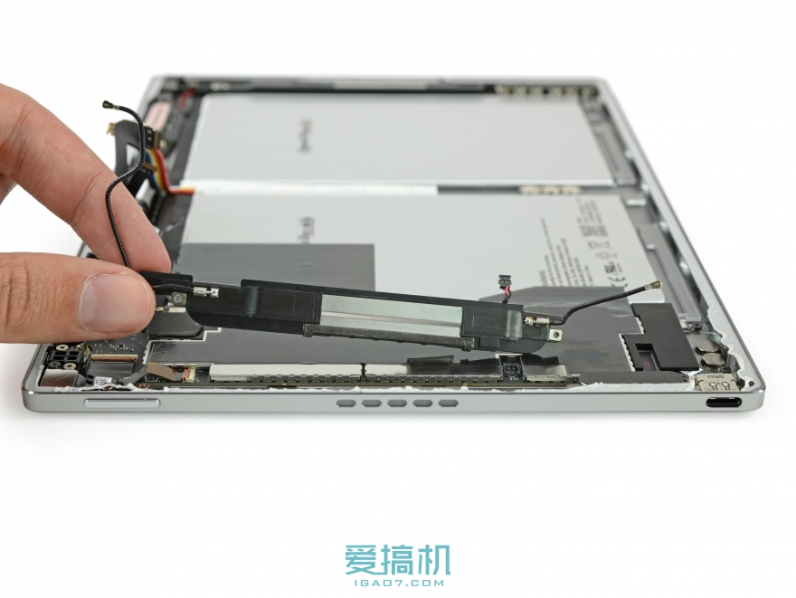
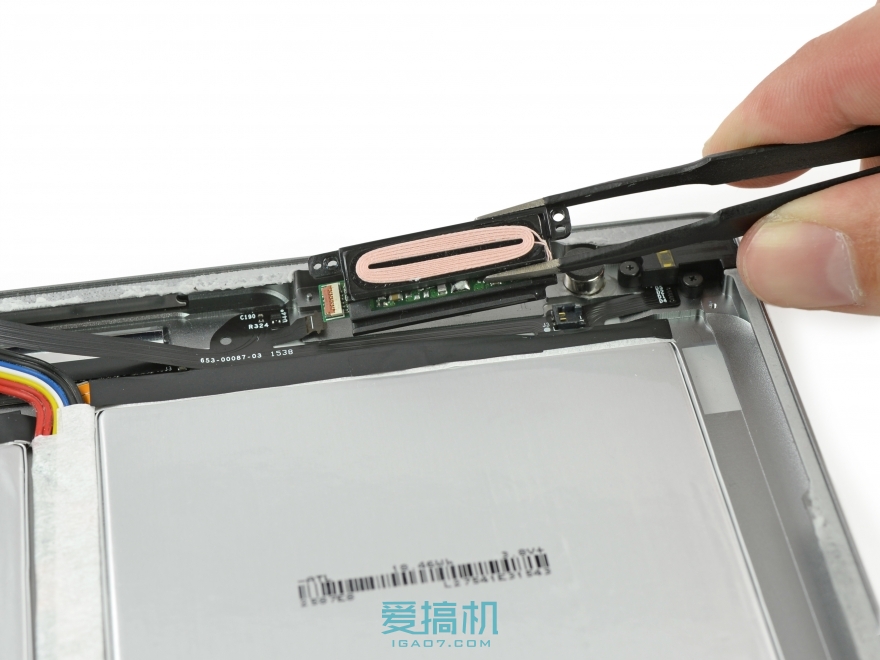
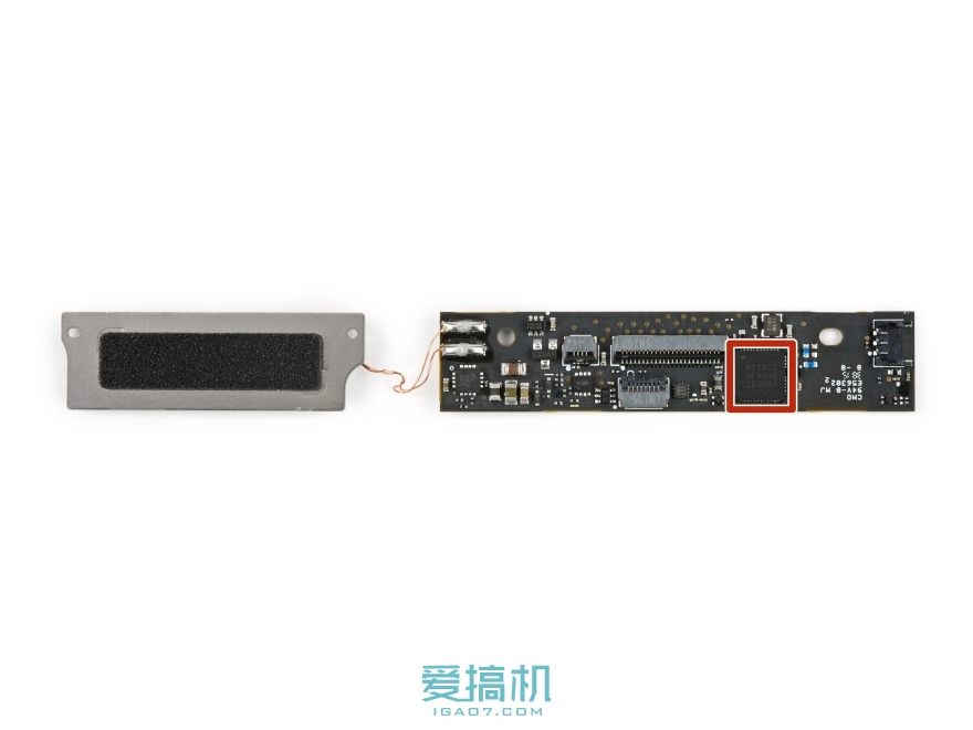
Then the built-in speakers were removed and three cables were connected to it.
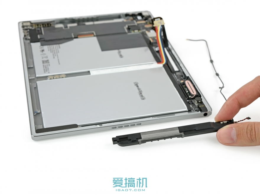
There is also a speaker on the other side of the fuselage. The cable length is relatively long. Be careful when removing it.
Then remove the USB Type-C module and only need a Phillips screwdriver.
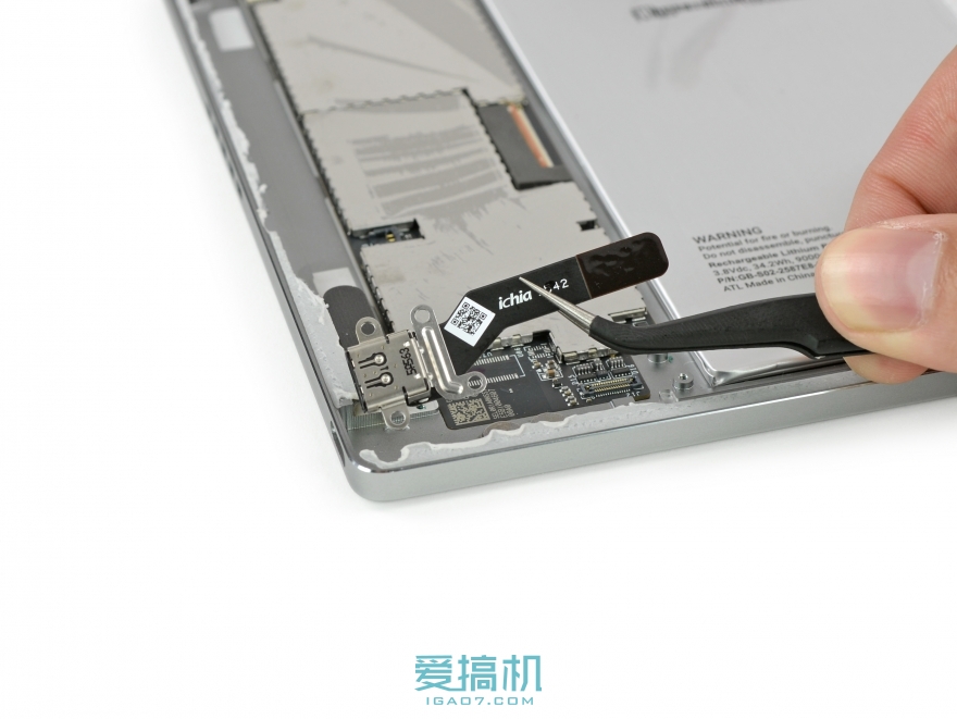
The USB Type-C interface adopts a modular design. After the screws are removed, unplugging the cables can be removed.
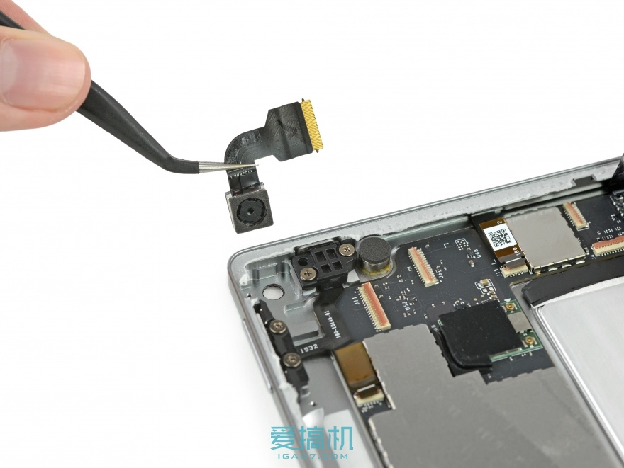
Then remove the rear camera and use the cable to fix it.

After removing the rear camera, you can remove the power button and volume button module.
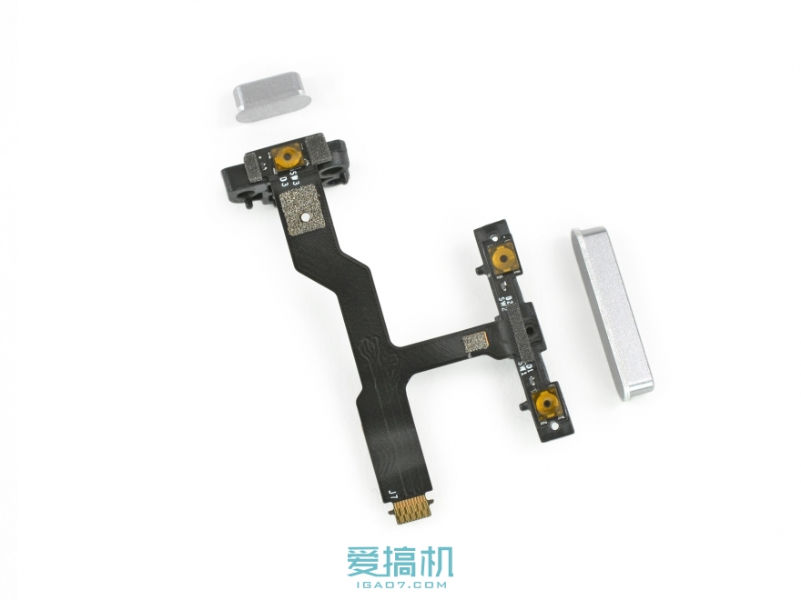
Power switch and volume button and all components. Both the power button and the volume button are simply fixed by screws, and removal and replacement are convenient.
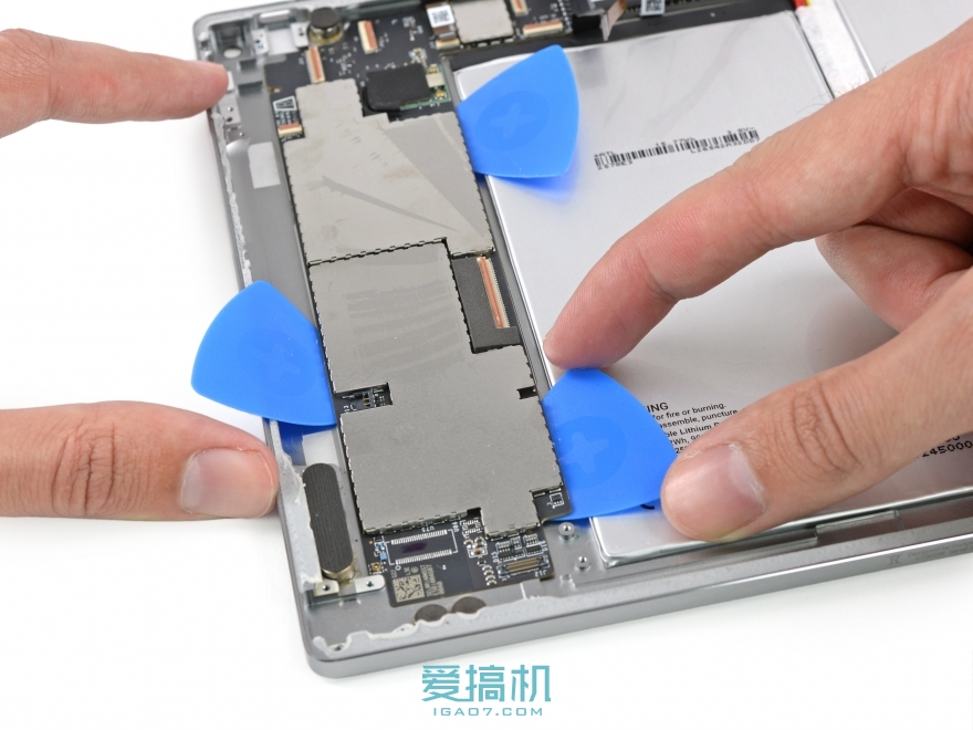
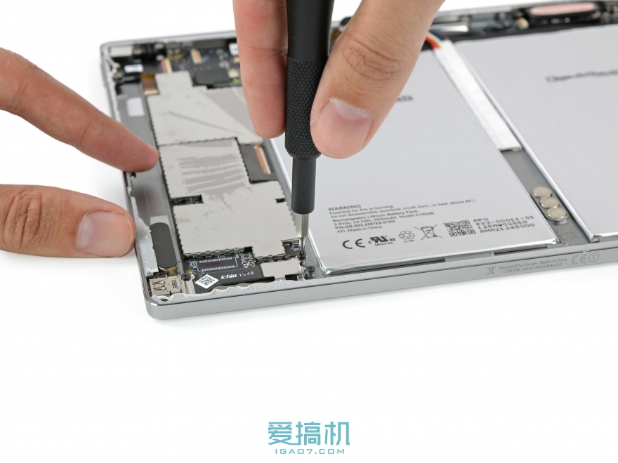
After disassembling the components, we can disassemble the mainboard. The mainboard area is very small and the integration is very high. The main board is glued to the back cover by glue. We use the paddle to slowly pull the board down along the edge of the main board. If it is difficult to remove, you can use a hot air gun to heat the motherboard.
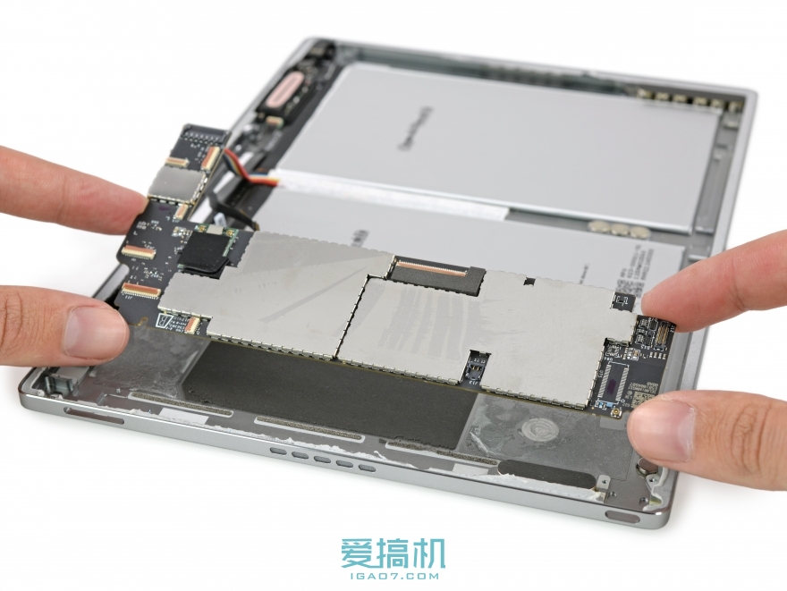
Now you can finally take out the motherboard. There is a large area of ​​adhesive and insulating foam under the main board.
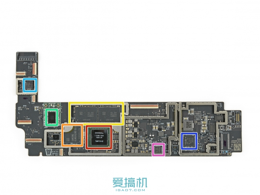
All the chips are located on the front of the main board. The back side is very clean with only solder joints. Let's see what chips are on the motherboard.
Red: Nvidia Tegra X1 64-bit quad-core processor
Orange: Samsung KLMBG4GEND 32 GB eMMC flash memory chip
Yellow: Samsung K4F2E304HMMGCH 6 Gbit LPDDR4 RAM chip capacity is 1.5 GB x 2 = 3GB
Green: Broadcom BCM43540LKUBG 5G Wi-Fi 802.11ac control chip
Light Blue: Nuvoton NAU88L25 Audio Codec
Dark blue: STMicroelectronics STM32F3x8 32-bit ARM Cortex-M4 microcontroller
Purple: Infineon SLB 9645 trusted platform module
After analyzing the motherboard, we take a look at the keyboard charging coil located at the bottom of the fuselage.
On the back of the charging coil there is a small circuit board that controls wireless charging. The circuit board should be the control module that controls the power supply of the coil to generate the electromagnetic field.
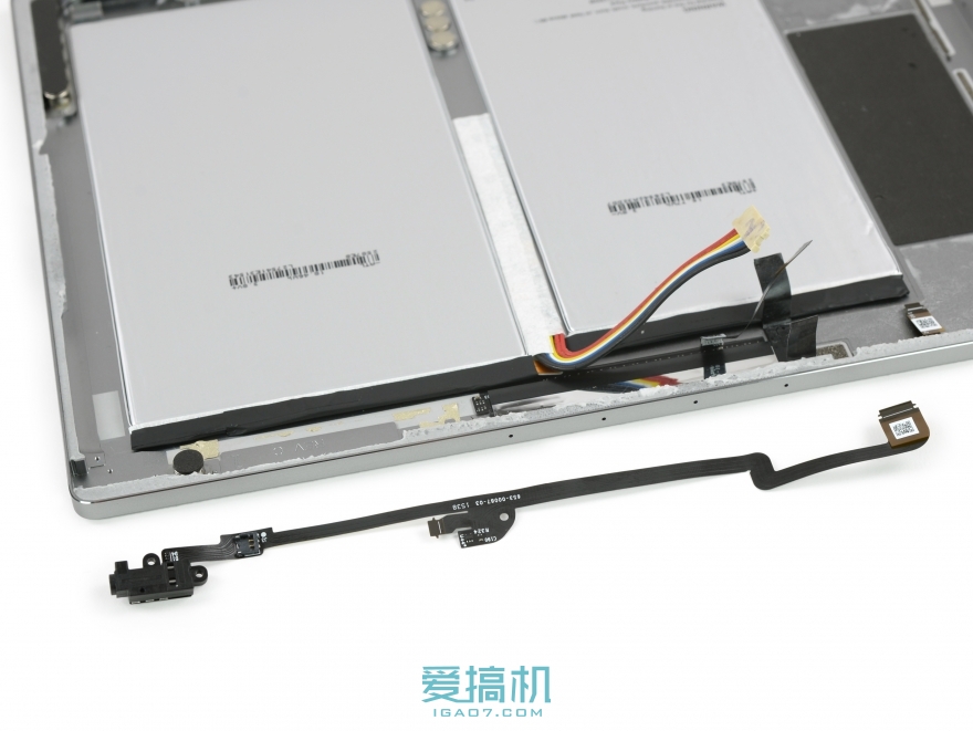
On the other side of the battery there is a 3.5 mm headphone jack, which is connected to the motherboard through a fairly long cable.
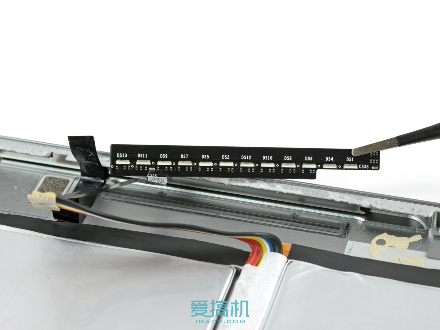
We accidentally found a display panel full of LED lights under the audio cable. This should be the backlight of the indicator light. The reflection on the surface of the fuselage will be illuminated by the reflection of the metal foil.

Finally, there are four noise-canceling microphones on the top of the fuselage.

The machine's built-in battery is 34.2 watt-hours, 27.9 watt-hours greater than the 9.7-inch iPad Pro, but slightly lower than the Surface Pro 4's 38.2 watt-hours.
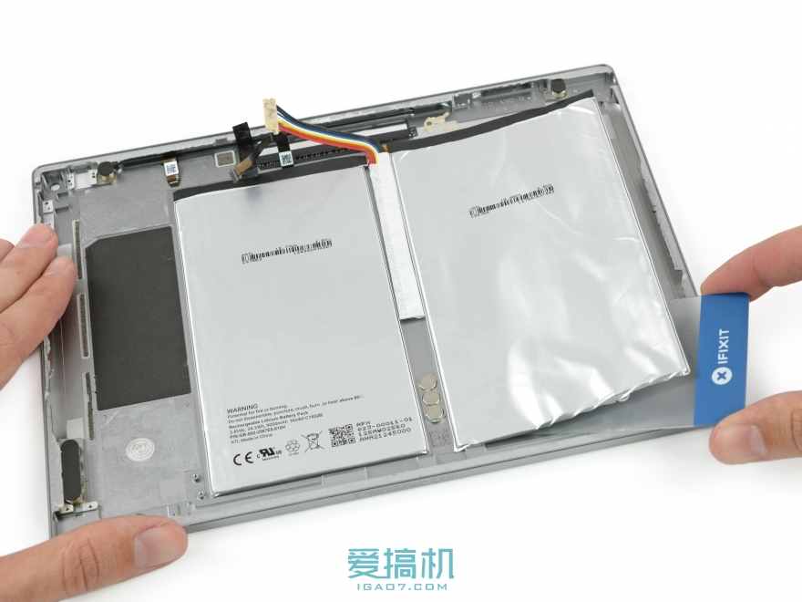
The glue on the back of the battery is very firm and it is very difficult to dismantle and it is still very strong after heating. The dismantling of the fuselage section ends here.
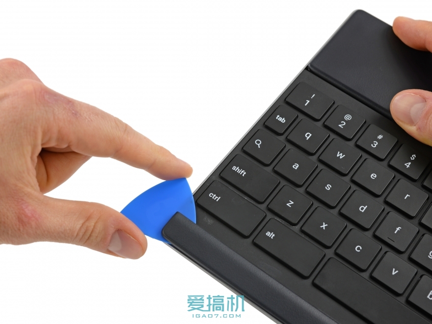
Next we will disassemble the matching Bluetooth keyboard. Remove the wrist from the bottom of the keyboard, heat it with a hot air gun, and slowly separate it with a paddle.

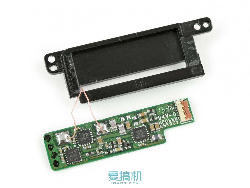
After removing the support arm, we can see the internal multiple magnets and inductive charging coils.

After disassembling the screws, use a hot air gun to evenly heat along the edges, and then use the paddle to slowly pick them up along the edges.
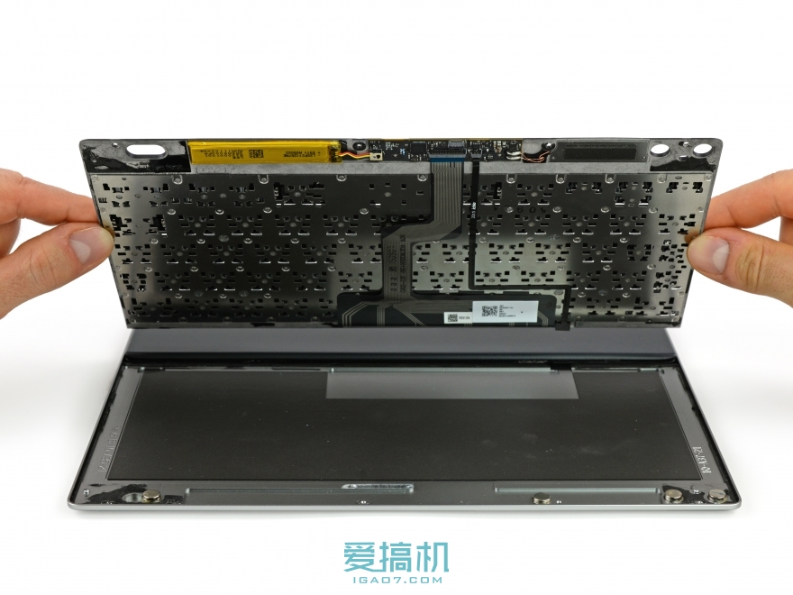
Then you can separate the keyboard from the base, and the steel plate at the bottom of the keyboard enhances the strength.

By analyzing the circuit and the cable, we believe that the keyboard is sensed by the Hall effect sensor to the tablet computer, and the tablet can be used immediately after it is recognized.
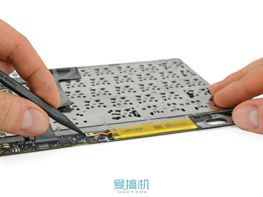
Then we can remove the built-in lithium-ion battery and connect it to the circuit board through the cable.
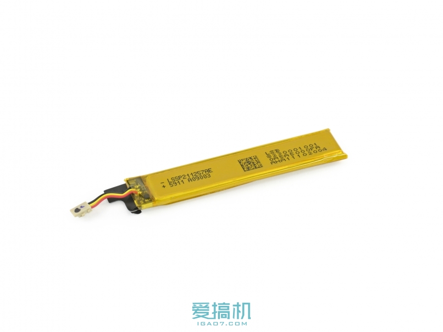
The built-in battery is very small and does not specify capacity. The keyboard is charged through the charging induction coil, but charging can begin when the keyboard is connected to the body.

Next we will take out the charging induction coil and motherboard.
The coils are soldered to the motherboard via wires. The core of the entire keyboard is the Nordic Semiconductor nRF51822 2.4 GHz Bluetooth module + 32-bit ARM Cortex-M0 microcontroller. Well, the dismantling of the keyboard has also been completed here.

At this point, our dismantling was all completed. iFixit scored 4 points (out of 10 points) for Pixel C's maintenance capabilities and scored relatively low. Most of the internal parts of the fuselage use a modular design, such as the USB Type-C interface, 3.5mm headphone jack, and power volume switch, which can be easily replaced. However, some designs are more difficult to dismantle and maintain. If the motherboard is very firmly bonded to the body, the battery is using a very sticky glue so that we can not successfully remove it, these designs will undoubtedly increase the difficulty of maintenance.