RF (Radio Frequency) technology is widely used in many fields, such as: television, radio, mobile phones, radar, automatic identification systems. The special word RFID (Radio Frequency Identification) refers to the application of radio frequency identification signals to identify the target. RFID applications include:
â— ETC (electronic charge)
â— Railway locomotive vehicle identification and tracking
â— Container identification
â— Identification, certification and tracking of valuables
â— Target management of commercial retail, healthcare, logistics services, etc.
â— Entry control
â— Animal identification, tracking
â— The vehicle is automatically locked (anti-theft)
RF (Radio Frequency) refers to electromagnetic waves that have a certain wavelength that can be used for radio communication. Electromagnetic waves can be expressed by their frequencies: KHz (kilohertz), MHz (MHz) and GHz (gigahertz). The frequency range is VLF (very low frequency), that is, 10-30 KHz to EHF (very high frequency), that is, 30-300 GHz.
RFID is a flexible application technology that is easy to handle, simple and practical, and especially suitable for automated control. Its unique superiority is beyond the reach of other identification technologies. It supports both read-only mode and read-write mode, and requires no contact or aiming; it can work freely in a variety of harsh environments; it can be highly integrated. In addition, because the technology is difficult to be counterfeited and invaded, RFID has a very high security protection capability.
Conceptually, RFID is similar to bar code scanning. For bar code technology, it attaches the encoded bar code to the target and uses a dedicated scanning reader to transmit information from strip magnet to scan read and write using optical signals. RFID uses a dedicated RFID reader and a dedicated RFID unit that can be attached to the target to transmit information from the RFID unit to the RFID reader using RF signals.
The RFID unit carries various types of related information about the target object, such as the name of the target object, the start and end point of the target transportation, the transit point, and the specific time when the target object passes through a certain place, etc., and can also load such as temperature. And other indicators. RFID units, such as labels, cards, etc., can be flexibly attached to various items from the vehicle to the cargo chassis.
The frequency of radio waves used in RFID technology is 50KHz-5.8GHz. As shown in Figure 1, a basic RFID system generally includes the following parts:
â— An RFID unit (answering machine or card, label, etc.) carrying information about the target
â— Antenna that transmits RF signals between readers and RFID units
â— An RF transceiver that generates RF signals
• A reader that receives the RF signal returned from the RFID unit and transmits the decoded data to the host system for processing.
â— Antennas, readers, transceivers, and mainframes can be partially or fully integrated into a single unit or integrated into a small number of components. Different manufacturers have different integration methods.
(In addition to the above basic configuration, the corresponding application software should also be included)
RF technology - typical RF circuit
The most important application area of ​​RF circuits is wireless communication. Figure 1 is a block diagram of a typical wireless communication system. The following uses this system as an example to analyze the role of RF circuits in the entire wireless communication system.
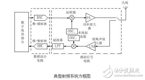
This is a system model of a wireless communication transceiver ("span" tranceiver) that includes a transmitter circuit, a receiver circuit, and a communication antenna. This transceiver can be used in personal communications and wireless local area networks. In this system, the digital processing part mainly processes the digital signal, including sampling, compression, encoding, etc.; then it becomes an analog form into the analog signal circuit unit through the A/D converter.
RF technology - the composition and characteristics of the circuitIn the following, the composition and characteristics of a general RF circuit will be discussed with respect to a low noise amplifier (LNA) in the block diagram of the figure.
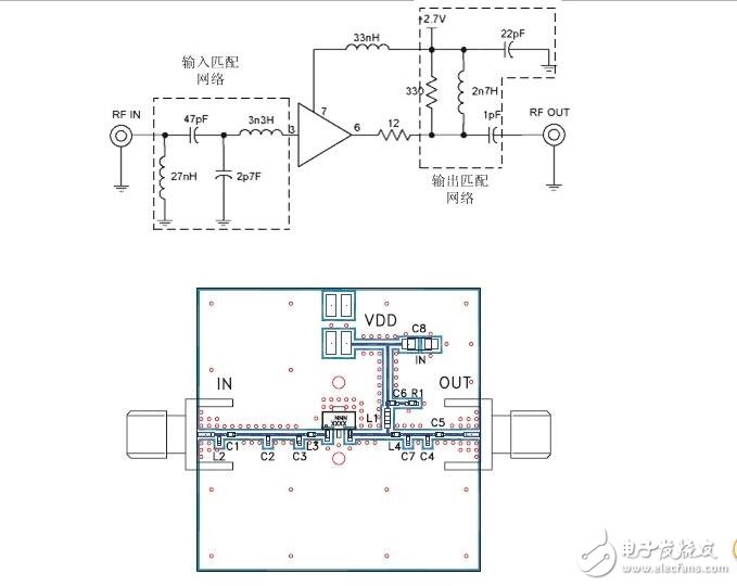
The figure above shows the board diagram of this amplifier, noting that the input signal is passed through a matched filter network input amplification module. The amplification module generally uses a common emitter structure of the transistor, and its input impedance must match the output impedance of the filter located in front of the low noise amplifier to ensure optimal transmission power and minimum reflection coefficient. For RF circuit design, this Matching is a must. In addition, the output impedance of the low noise amplifier must match the mixer input impedance at the back end, as well as ensuring that the amplifier output signal is fully and non-reflective input to the mixer. These matching networks are composed of microstrip lines and sometimes may be composed of independent passive components, but their electrical characteristics at high frequencies are quite different from those at low frequencies. It can also be seen that the microstrip line is actually a copper strip of a certain length and width, and the microstrip line is connected with a chip resistor, a capacitor and an inductor.
RF Technology - Power and Gain of CircuitsGain, noise, and nonlinearity are the most commonly used indicators for describing RF circuits. In RF and microwave systems, the measurement of voltage and current parameters commonly used in low frequency circuits becomes very difficult due to the ubiquity of reflection and the ideal short circuit and open circuit. Therefore, power measurement has been widely used. Moreover, conventional RF and microwave circuits are constructed using discrete components and transmission lines. The input and output of the circuit typically need to be matched to a system impedance (50? or 75?). For the above two reasons, the performance indicators of the circuit, such as gain, noise, nonlinearity, etc., can be expressed by power.
For the convenience of calculation, power is used in the form of logarithm of power intensity in RF and microwave engineering, and dBm is the logarithm of signal power with respect to 1 mW.
With the definition of power, it is now time to discuss an important indicator in the RF system: gain. The power considered in the RF system refers to the power gain, which is easily confused with the voltage gain. In addition, in the RF system, there are also multiple power definitions. When the matching circuit is present, the following power can be defined:
PL: power obtained by the load
Pin: input power of the circuit
Pavs: the maximum power that the source can provide
Pavn: the maximum power that the circuit can provide
Accordingly, three types of power can be defined: a general power gain Gp, a converted power gain GT, and a capital gain GA, which are given by the following equations.
   RF technology - circuit design methodWireless transmitters and receivers are conceptually divided into two parts: the fundamental frequency and the radio frequency. The fundamental frequency contains the frequency range of the transmitter's input signal and also the frequency range of the receiver's output signal. The bandwidth of the fundamental frequency determines the basic rate at which data can flow through the system. The fundamental frequency is used to improve the reliability of the data stream and to reduce the load imposed by the transmitter on the transmission medium below a specific data transmission rate. Therefore, when designing a baseband circuit for a PCB, a large amount of signal processing engineering knowledge is required. The transmitter's RF circuitry converts, upconverts, and upconverts the processed baseband signal into a designated channel and injects this signal into the transmission medium. Conversely, the receiver's RF circuit can take signals from the transmission medium and convert and down-convert them to the fundamental frequency.
The transmitter has two main PCB design goals: the first is that they must emit as much power as possible while consuming the least amount of power. The second is that they cannot interfere with the normal operation of the transceivers in adjacent channels. As far as the receiver is concerned, there are three main PCB design goals: first, they must accurately restore small signals; second, they must be able to remove interfering signals outside the desired channel; the last point, like the transmitter, they must consume the power Very small.
RF technology - large interference signalsThe receiver must be sensitive to small signals, even when large interfering signals (barriers) are present. This occurs when an attempt is made to receive a weak or long-range transmit signal, with a powerful transmitter nearby broadcasting in an adjacent channel. The interference signal may be 60~70 dB larger than the expected signal, and may block the reception of the normal signal by a large amount of coverage in the input phase of the receiver or by causing the receiver to generate excessive noise during the input phase. If the receiver is in the input phase and the interferer drives the non-linear region, the above two problems will occur. To avoid these problems, the front end of the receiver must be very linear.
Therefore, "linear" is also an important consideration when designing a receiver for a PCB. Since the receiver is a narrowband circuit, the nonlinearity is measured by measuring "intermodula distortion". This involves using two sine or cosine waves of similar frequency and located in the center band to drive the input signal and then measure the product of its alternating modulation. In general, SPICE is a time-consuming and costly simulation software because it has to perform many loop operations to get the required frequency resolution to understand the distortion.
The receiver must be sensitive to detect small input signals. In general, the receiver's input power can be as small as 1 μV. The sensitivity of the receiver is limited by the noise generated by its input circuitry. Therefore, noise is an important consideration when designing a receiver for a PCB. Moreover, the ability to predict noise with simulation tools is indispensable. Figure 1 is a typical superheterodyne receiver. The received signal is filtered first and then amplified by a low noise amplifier (LNA). This signal is then mixed with this signal using the first local oscillator (LO) to convert this signal to an intermediate frequency (IF). The noise performance of the front-end circuitry is primarily dependent on the LNA, mixer, and LO. Although the noise of the LNA can be found using conventional SPICE noise analysis, it is useless for the mixer and LO because the noise in these blocks is severely affected by the large LO signal.
A small input signal requires the receiver to have a very large amplification function, which typically requires a gain of 120 dB. At such high gains, any signal that is coupled back to the input from the output can cause problems. An important reason for using a superheterodyne receiver architecture is that it distributes the gain across several frequencies to reduce the probability of coupling. This also makes the frequency of the first LO different from the frequency of the input signal, preventing large interfering signals from "contaminating" to small input signals.
For some different reasons, in some wireless communication systems, a direct conversion or homodyne architecture can replace the superheterodyne architecture. In this architecture, the RF input signal is directly converted to the fundamental frequency in a single step, so most of the gain is in the fundamental frequency and the LO is the same frequency as the input signal. In this case, the influence of a small amount of coupling must be known, and a detailed model of the "stray signal path" must be established, such as coupling through the substrate, package pins and bond wires. Coupling between (bondwire) and coupling through the power line.
RF technology - interference from adjacent channels in circuit simulationDistortion also plays an important role in the transmitter. The non-linearity produced by the transmitter in the output circuit may spread the bandwidth of the transmitted signal in adjacent channels. This phenomenon is called "spectral regrowth." Before the signal reaches the power amplifier (PA) of the transmitter, its bandwidth is limited; however, the "intermodulation distortion" in the PA causes the bandwidth to increase again. If the bandwidth is increased too much, the transmitter will not be able to meet the power requirements of its neighboring channels. When transmitting a digital modulation signal, in fact, SPICE cannot be used to predict the re-growth of the spectrum. Since approximately 1000 digital symbol transfer operations must be simulated to obtain a representative spectrum and also need to be combined with high frequency carriers, these will make SPICE transient analysis impractical.
- The Description of wifi Antenna
-
When selecting the antenna, it is necessary to pay attention to whether the connector of the antenna matches the connector of the connected device. Generally, SMA and TNC are used for WIFI
To use on the router, but on the 2.4 G wireless monitoring equipment fittings, if match, also can achieve the enhancement effect of the wireless signal transmission Magnetic antenna base, can suck on metal surfaces, makes the antenna signal is stronger Plug and play, without any additional conditions, but the antenna gain and directional property management are key points to consider. - The first standard WIFI antenna products were made by LTCC process, because of its width and general performance. Abroad, Airgain has launched a standard antenna with high temperature resistance and plastic seal, which is used in laptop computers, and a series of WiFi antennas with magnetic dielectric in mobile phones have been launched in China.
- The Picture of wifi Antenna
-

Wifi Antenna ,Wifi Antenna for PC ,Wifi Antenna for Router ,Wfi Antenna outdoor ,Wifi Antenna Indoor
Yetnorson Antenna Co., Ltd. , https://www.yetnorson.com