Freescale's MC33903 / 4/5 is the second-generation system foundation chip (SBC), which can be used as an advanced power management for MCUs, and integrates several advanced integrated circuits such as sensors and CAN transceivers, and has an enhanced high-speed CAN interface. (ISO11898-2 and -5), as well as local and bus fault diagnosis, protection and fail-safe operation modes. Mainly used in aviation and underwater systems, automotive and robotic systems, farm equipment, light and inductive load control, DC motor control, Industrial excitation control, etc. This article introduces the main features of MC33903 / 4/5 series products, block diagrams and simplified application block diagrams, the main features of the evaluation board KIT33905D5EKEVBE, the establishment of block diagrams, circuit diagrams, bill of materials and PCB component layout and wiring diagrams.
The 33903/4/5 is the second generaTIon family of the System Basis Chip (SBC). It combines several features and enhances present module designs. The device works as an advanced power management unit for the MCU with addiTIonal integrated circuits such as sensors and CAN transceivers. It has a built-in enhanced high-speed CAN interface (ISO11898-2 and -5) with local and bus failure diagnosTIcs, protecTIon, and fail-safe operation modes. The SBC may include zero, one or two LIN 2.1 interfaces with LIN output pin switches. It includes up to four wake-up input pins that can also be configured as output drivers for flexibility. This device is powered by SMARTMOS technology.
This device implements multiple Low-power (LP) modes, with very low-current consumption. In addition, the device is part of a family concept where pin compatibility adds versatility to module design.
The 33903/4/5 also implements an innovative and advanced fail-safe state machine and concept solution.
• Voltage regulator for MCU, 5.0 or 3.3 V, part number selectable, with possibility of usage external PNP to extend current capability and share power dissipation
• Voltage, current, and temperature protection
• Extremely low quiescent current in LP modes
• Fully-protected embedded 5.0 V regulator for the CAN driver
• Multiple undervoltage detections to address various MCU specifications and system operation modes (ie cranking)
• Auxiliary 5.0 or 3.3 V SPI configurable regulator, for additional ICs, with overcurrent detection and undervoltage protection
• MUX output pin for device internal analog signal monitoring and power supply monitoring
• Advanced SPI, MCU, ECU power supply, and critical pins diagnostics and monitoring.
• Multiple wake-up sources in LP modes: CAN or LIN bus, I / O transition, automatic timer, SPI message, and VDD overcurrent detection.
• ISO11898-5 high-speed CAN interface compatibility for baud rates of 40 kb / s to 1.0 Mb / s
• Scalable product family of devices ranging from 0 to 2 LINs which are compatible to J2602-2 and LIN 2.1
MC33903
• Aircraft and marine systems
• Automotive and robotic systems
• Farm equipment
• Industrial actuator controls
• Lamp and inductive load controls
• DC motor control applications requiring diagnostics
• Applications where high-side switch control is required
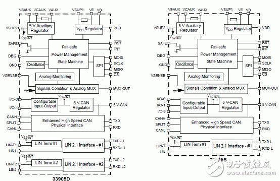
Figure 1. Internal block diagram of MC33905
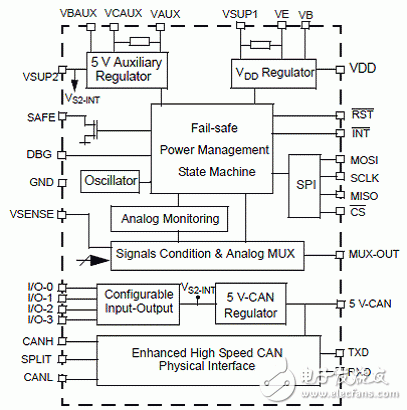
Figure 2. Internal block diagram of MC33904
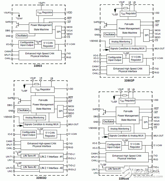
Figure 3. Internal block diagram of MC33903
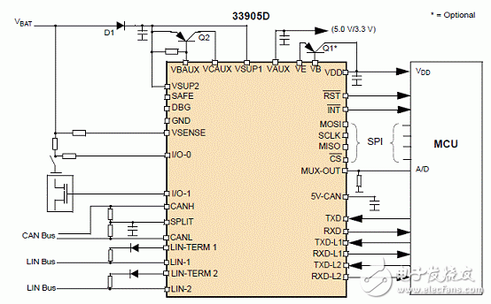
Figure 4. MC33905D simplified application block diagram
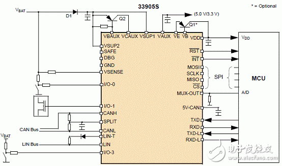
Figure 5. Simplified application block diagram of MC33905S
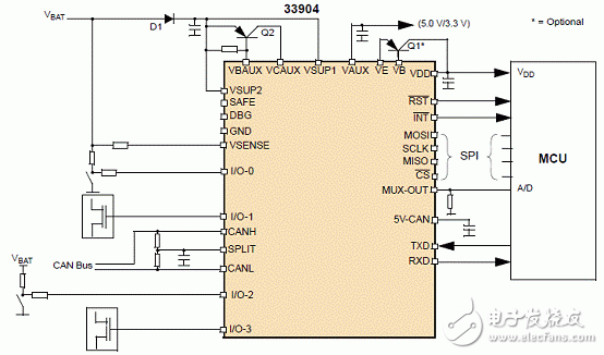
Figure 6. MC33904 simplified application block diagram
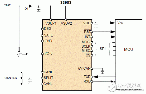
Figure 7. MC33903 simplified application block diagram
The KIT33905D5EKEVBE supports the 33905D5 and 33904 devices, which are the second generation family of System Basis Chips, which combine several features and enhance present module designs. The devices work as an advanced power management unit for the MCU and additional integrated circuits such as sensors, CAN transceivers. They have a built-in enhanced high speed CAN interface (ISO11898-2 and -5), with local and bus failure diagnostics, protection, and fail safe operation mode. The SBCs may include one or two LIN 2.0 interfaces with LIN output pin switches. The 33904/5 include 2 or 3 wake-up input pins than can also be configured as output drivers for flexibility.
Nominal operating supply voltage range of 5.5 V to 27 V
Individually routed power supply inputs for VSUP1 and VSUP2
5.0 / 3.3 V regulator for MCU with an external PNP ballast transistor to increase current capability
Multiple CAN Bus termination options supported via socket
Two high / low side I / Os (SPI configurable) accessible through test points
Status of I / O-0 and I / O-1 indicated by an LED (dependent on jumper configuration)
Debug mode / watchdog configuration via jumper settings
MUX output voltage accessible through a test point and external resistor selectable through jumper
3.3 V or 5.0 V output voltage test point VAUX (SPI configurable)
I_WAKE_I test point to enable a FET and load VDD with current to wake-up the SBC
LIN1_T and LIN2_T test points to monitor I / O voltages (SPI configurable)
I / O-0, I / O-1, VAUX, 5V_CAN, SAFE, and VDD status indicated by LED
100 mil 2x8 pin standard header connector for SPI communication
100 mil 16 pin standard header connector for custom MCU board connections
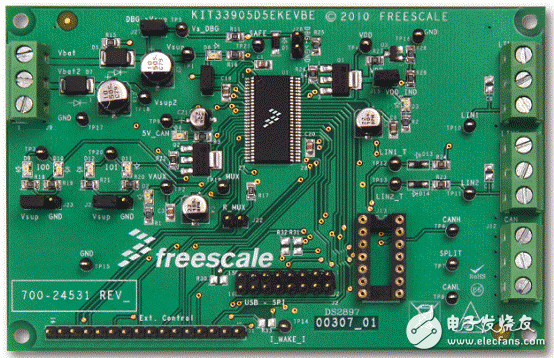
Figure 8. Evaluation board KIT33905D5EKEVBE / KIT33905BD3EVBE outline drawing
• KIT33905D5EKEVBE or KIT33905BD3EVBE Hardware
• CD33905 (includes SPIGen Software)
• CABLE, RIBBON FLAT 16 PIN ASSY, 0.100 "PITCH, 6" LENGTH
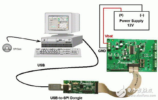
Figure 9. Evaluation board KIT33905D5EKEVBE / KIT33905BD3EVBE setup configuration diagram
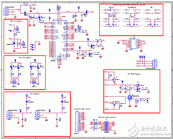
Figure 10. Evaluation board KIT33905D5EKEVBE circuit diagram
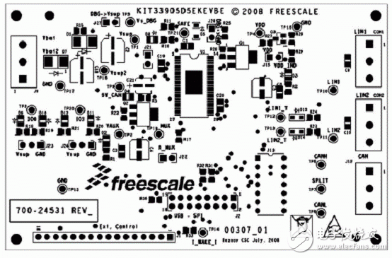
Figure 11. Layout of the top-level PCB components of the evaluation board KIT33905D5EKEVBE
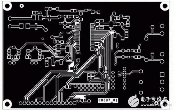
Fig. 12. Evaluation board KIT33905D5EKEVBE top-level PCB wiring diagram
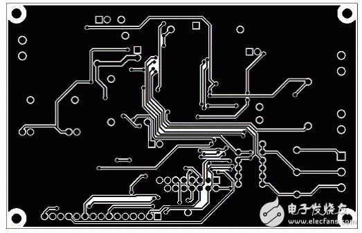
Figure 13. Evaluation board KIT33905D5EKEVBE bottom PCB wiring diagram
0.8mm Pin Header
Antenk 0.8mm Pitch Male Header series is a fine pitch, low profile, single/dual/three/four row, PCB mounted connector set intended for limited space applications or where total weight is a factor. Our specially tooled insulators and contacts maintain consistent high quality through our automated production processes. Each series is available in thru-hole PCB or SMT mounting and plated tin, gold or selective gold as specified.
0.8mm Pin Header Options
Number of Rows
1/Single
2/Double
3/Three
4/Quad
Number of Positions
2 Position
3 Position
4 Position
5 Position
6 Position
8 Position
10 Position
12 Position
14 Position
15 Position
16 Position
17 Position
20 Position
Termination Style
SMD/SMT
Through Hole
Mounting Angle
Right Angle
Straight
0.8mm Pin Header Specifications:
Material: Standard Hi-Temp insulator: Nylon 6T, rated UL94V-0
Insulator Color: Black
Contacts: Phosphor Bronze
Plating:
U = Gold over nickel underplate
SG = Gold over nickel underplate on
contact area, tin over copper underplate on tails.
T = Tin over copper underplate overall.
Electrical:
Operating voltage: 250V AC max.
Current rating: 1 Amp max
Contact resistance: 20 mΩ max. initial
Insulation resistance: 5000 MΩ min.
Dielectric withstanding voltage: 1000V AC for 1 minute
Mechanical:
Mating durability: 500 cycles min.
Temperature Ratings: Operating temperature: -40°C to +105°C
Max process temp: 230°C for 30 ~ 60 seconds (260°C for 10 seconds)
Soldering process temperature: 260°C
Packaging:
Anti-ESD plastic bags or tubes
Approvals and Certifications:
UL Recognized File no. E224053
Pin Header,0.8Mm Male Header,0.8Mm Pin Header,0.8Mm Male Header Pins,0.8mm Pitch Pin Header,SMT 0.8mm Pin Header, THT 0.8mm Pin Header
ShenZhen Antenk Electronics Co,Ltd , https://www.antenksocket.com