The mobile TV reception front end must have the sensitivity required to operate away from the transmitter and tolerate overload when there is a strong signal. Can be integrated into in-vehicle entertainment (ICE) systems, as well as mobile TV reception capabilities in a variety of portable electronic devices such as cell phones, portable digital assistants (PDAs), laptops, etc., even when the distance between the user's receiver and transmitter is There should also be good performance under the conditions of the itinerary (different from traditional broadcast TV). Combining a high-gain, low-noise amplifier (LNA) with a PIN diode bypass switch provides a low-cost solution for mobile TV receiver front ends with overload protection and high sensitivity.
This article refers to the address: http://
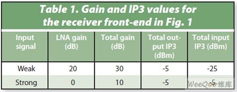
Table 1: Gain and IP3 of the receiver front end shown in Figure 1.
The most practical way to implement a mobile TV receiver is to reduce the gain of the receiver under strong signal conditions. The variable RF signal gain simplifies the linearity requirements of the mixer stage, allowing the use of low cost RF ICs to build the receiver module. In a cascade analysis with a switchable/tunable gain receiver front end, the improvement in the input third-order intercept point (IIP3) will be a function of gain variation (see Figure 1 and Table 1). The adjustable gain receiver is better able to handle strong signals than fixed gain receivers.
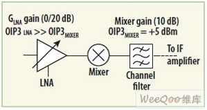
Figure 1: Simplified block diagram of the receiver front end with variable gain LNA stage.
The Automatic Gain Control (AGC) circuit can also be used to change the LNA gain, and since the AGC is typically implemented before the channel filter, it can respond to overloads from adjacent channel transmissions.
One way to reduce the RF gain is to shunt some of the RF signal to ground before the LNA, see Figure 2(a). This method uses the least number of RF switching elements, but when the switch is turned off, the impedance is mismatched, which may affect other parts of the system. A workaround is to connect the damper element to the high impedance or "hot" end of the LNA parallel resonant network, although this approach sacrifices RF selectivity prior to the LNA from a larger gain control range.
When the received signal is overloaded to the stages behind the LNA, such as a mixer or intermediate frequency (IF) amplifier, the LNA stage can also be bypassed by means of a pair of RF switches. In the bypass state, the input signal is sent directly to the downconverter IC, see Figure 2(b). As long as the devices in the bypass signal loop match the characteristic impedance (mobile TV is 75Ω), the chance of mismatch is minimized. Of course, the added switch makes the circuit more complicated.
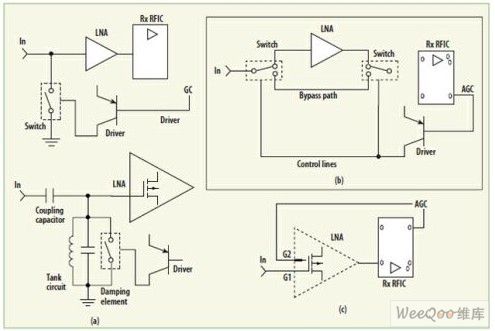
Figure 2: Gain control: (a) LNA input attenuation; (b) LNA bypass switch; (c) Gate bias modulation.
Another approach is to reduce the RF gain by reducing the quiescent current of the active device supplied to the LNA, see Figure 2(c). Amplifiers and devices using this technology, such as dual-gate MOSFETs, use additional device terminations to control the bias current. Since the switching element is not used, this gain control method is the simplest on the circuit, but its linearity is sacrificed because the collector/drain current is lower than the rated device DC operating point.
In order to meet the customer's LNA requirements for dual-mode (analog/digital) mobile TV receivers operating in the 47-870 MHz spectrum, several MMIC options have been considered (Table 2), but their linearity is not good enough, so they are not use. A broadband high-linearity MMIC LNA (MGA-68563) and an external PIN diode switch are used to design a solution.

This single-stage GaAs PHEMT LNA device has a gate width of 800 microns (Figure 3). The device's gate is connected to an internal current mirror to complement the effects of process variations and minimize the effects of threshold voltage variations. The LNA uses lossy negative feedback to achieve stability and smooth the amplitude response in a 3dB window (±1.5dB) in the 100MHz~1GHz spectrum.
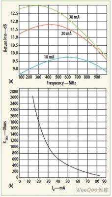
The MMIC does not require output impedance matching due to its internal feedback and output return loss of less than 10 dB. But matching the inputs over such a wide frequency range (47~870MHz) proves to be not an easy task and requires an unconventional approach where the FET's drain current (Ids) is high to optimize the input return loss specification. The nominal value is 10 mA. The 20 mA Ids meet the input return loss performance requirements, but the Ids is chosen to be 30 mA to make it sufficiently wide to compensate for any effects of the increased PIN diode switching circuitry. Pin 4 of the MMIC LNA controls the current flowing through the internal bias current generator via an external resistor R1 (Figures 3(a) and 4(b)). Changing the size specification of R1 will change the Ids, but the supply voltage Vd will remain at 3V. Increasing the nominal Ids by a factor of three provides greater linearity.
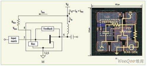
Figure 3: Simplified equivalent circuit (a) of the MGA-68563 MMIC LNA(b).
When designing the LNA/switch circuit, the first bypass switch (Fig. 5(a)) uses four PIN diodes. This is a common configuration for double pole double throw (DPDT) switches. The circuit works by turning the PIN diode pair at the top to be turned on, so that the lower pair is biased to zero and vice versa. In normal operation, only the low pair of PIN diodes are turned on, and the LNA amplifies the RF signal. When the RF gain must be reduced, the upper pair of PIN diodes are turned on and the RF signal is routed around the LNA in bypass mode. These resistors are used to regulate the forward current of the PIN diode and to isolate the RF signal from the logic control ports VSW1 and VSW2. The first design used a lot of components, so look for a simpler solution.
By communicating with our customers, we have developed a simpler double-pole single-throw (DPST) switch (Fig. 5(b)) that simply connects or disconnects the bypass path to the input and output ports. Since the switching control of the LNA path is no longer performed, in order to utilize the inherent isolation characteristic of the unbiased FET, the LNA power supply (Vdd) must be turned off in the bypass mode. This approach reduces the return loss performance of the bypass path because it has a finite gate and drain impedance in which the unbiased FETs are connected in parallel.
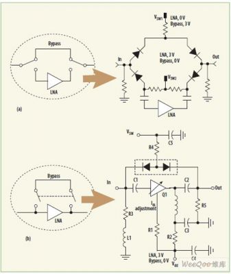
Figure 5: (a) The originally designed switching circuit has 4 PIN diodes; (b) The modified circuit has only 2 PIN diodes.
In normal operation, the PIN diode power is turned off (VSW = 0V) and the LNA power supply is still restored to 3V. However, these zero-biased PIN diodes are subject to parasitic capacitance, so the gain and return loss performance of the LNA is compromised by incomplete isolation of the bypass path from the input and output ports.
Within the LNA/switch, inductors L1 and L2 are ferrite beads that exhibit high impedance over the entire range of MMIC and diode bias networks (Figure 5(b)). Without L1 as the choke, a portion of the input signal will be bypassed to ground through a parasitic capacitance in parallel with resistor R3. Measurements made on a prototype board without L1 show that the inductor prevents deterioration of the LNA noise figure. Capacitors C3, C4, and C5 decouple the RF signals from the DC source, and their capacitive reactance values ​​are small (Xc is 5Ω at the lowest operating frequency). Capacitors C1 and C2 act as a direct barrier at the input and output of the MMIC. C2 is deliberately chosen to be a small value to produce a high-pass response that compensates for the inherent gain-roll-off characteristics of the MMIC at high frequencies. Resistors R1 and R2 control the current of the MMIC, which makes the current 30 mA when Vdd = 3V. At VSW = 3V, resistors R3, R4, and R5 limit the forward bias of the PIN diode to approximately 2.5 mA.
This circuit can be further simplified with only one PIN diode, but there is no benefit to this because the SOT-23 or SOT-323 surface-mount diode pairs have the same footprint as a single diode, and the price difference is negligible. .
To estimate the performance of the LNA/switch, a prototype was previously built on a board designed for non-bypass NNA applications. The PCB consists of Rogers' RO4350B laminate. When the frequency is 10 GHz, the dielectric constant in the z direction is 3.48. The PIN diode and its associated biasing component are soldered directly to the pins/pads of the components previously present on the PCB. Two 1N5719 axial glass diodes are used as the switching elements of D1. In later PCB layouts, these diodes will be replaced with PIN diode pairs (HSMP-3893/E type) in SOT packages.
The median gain of the LNA is 19.8 dB ± 1.3 dB in the frequency range we are concerned with (Fig. 6(a)). By means of the high-pass response of the DC blocking capacitor C2, the signal with a frequency lower than 200MHz is moderately attenuated, ensuring a flat frequency response. The roll-off of the high-frequency gain is consistent with the characteristics of the MMIC and may result from the negative feedback of the parasitic capacitance of the unbiased PIN diode.
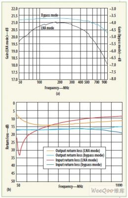
In bypass mode, the circuit has an attenuation of 3.8 to 4.5 dB over the entire spectrum (Figure 6(a)). The loss in this mode is mainly due to the parasitic series inductance of the PIN diode. The dissipation of the PCB, the FET termination impedance of the FET, and the parasitic shunt capacitance of resistor R4 have some effect on the loss of the bypass mode. However, the bypass mode loss is well controlled within the -5 dB level defined by the customer specification, so attempts are currently being made to further reduce the bypass loss.
When the bypass mode is evaluated over a specific frequency range, the input and output return loss performances are consistently good (less than 17 dB). The proximity of the gate and drain of the unbiased FET to the open-loop circuit is a major factor affecting the return loss. When the LNA is operating, the return loss performance is not as good, and the worst case at the lowest frequency is that the output return loss is equal to 7 dB. Below 70MHz, the poor output return loss performance is caused by the small value capacitor C2, which is a compromise for better frequency response.

Figure 7(a) compares the LNA noise figure with or without ferrite bead inductor L1. If there is no L1, the target noise specification (not higher than 1.3dB) cannot be met. By comparing the curves, it can be inferred that the parasitic capacitance of R3 has an effect on the signal loss of 0.3~0.6dB, which increases the noise by 0.3~0.6dB. If L1 is used, the in-band noise specification will change more (from 0.2dB to 0.5dB), but this is not important. These changes may be due to the increased turbulence of the ferrite bead as the frequency increases, especially for the self-resonant frequency (SRF) above about 100 MHz estimated from the performance chart provided by the manufacturer. This is the case.
In the mobile TV frequency band, the output third-order intercept point (OIP3) of the LNA is measured as a number of uniformly distributed frequency points using a two-tone input power level of -20 dBm. IIP3 was calculated by subtracting the gain measured from the OIP3 data. The OIP3 is not less than 30.3 dBm, and the maximum gain variation in the band is 0.8 dB (Fig. 7(b)). There is a 10dB improvement in the nominal value (20dBm) on the linear ratio data sheet, which can be attributed to the higher Ids used in the design.
The LNA/switch design meets its target specifications and shows tremendous potential for improvement. For example, noise performance can be improved by replacing the currently used products with higher ferrite bead inductors with SRF.
It can be equipped with different type of storage battery such as lead acid battery, Nickel Cadmium Battery, silver zinc battery, Lithium Ion Battery and other storage batteries, providing various output voltage classes.
Built-in storage battery and charger, equipped with the function of over-charge and over-discharge protection and capacity display. It is used as working power supply for lightings, communications, laptops, and special instruments of emergency working, field working, press interviews, special vehicles and other fields.
48V Dc Power Supply,Universal Power Supply,Power Supply 500W,Electrical Load Power Supply
Xinxiang Taihang Jiaxin Electric Tech Co., Ltd , http://www.chargers.be