l Introduction
With the rapid development of chip technology, a new generation of smart electronic products with light weight and small size are constantly coming out, and the packaging density requirements for electronic packaging are becoming higher and higher. Multi-chip mode (MCM, Muiti-ChipModuie) is one of them. solution. It is a technology that integrates two or more chips together. In order to effectively utilize the area of ​​the substrate material, the chip is often attached to different positions of the substrate by a COB (Chip on Board) mounting method. Since the residual stress caused by the package will directly affect the performance and service life of the chip, it is necessary to understand the residual stress at different positions on the organic substrate material. Reports related to this aspect have not been found at home and abroad. In addition, piezoresistive sensing is most suitable for real-time monitoring [ 2 - 4 ] compared to other methods such as laser interferometry [ l ] and X-ray diffraction. This study will study the residual stress on the surface of the chip pasted at different locations, and measure the stress change process during the heat treatment in situ.
2 Experimental principle, scheme and device
Figure 1 is a schematic view of the (111) plane of silicon. The n-type silicon piezoresistive sensing chip based on this surface was used in the experiment. According to the relevant piezoresistive theory, the mechanical calculation formula of plane stress solution is used [2], where Oij is the stress component, B1 and B2 are mutually independent piezoresistive coefficients, and R1, R2, R3 and R4 represent φ = 45° respectively. , 90 °, 135 °, 180 ° resistance values ​​in four directions, △ R represents the difference in resistance under stress and no stress.

Figure 1 (111) silicon wafer
The chip size of the Si (111)-faced n-type piezoresistive sensor used in the experiment was 6. 6 mm X 6. 6 mm X 1. 35 mm (see Fig. 2). There are five test points (A, B, C, D, E) on the chip. Each test point has eight sets of resistors that extend in eight directions to sense the resistance change in different directions. The resistance test uses a multi-channel real-time test system consisting of a Keithiey 2001 multimeter controlled by a microcomputer and its built-in scan card.

Figure 2 Silicon piezoresistive sensor chip for testing
In the experiment, the substrate material was made of FR4 (epoxy fiber cloth-clad copper foil laminate) material widely used in the electronics industry. The size of the selected substrate is 40mm X 40mm X 1mm. The chips are respectively attached to the center position of the two substrates, the position close to one side and the position close to one corner, which are respectively designated as 1, 2 and 3 (see Fig. 3). It should be noted that the substrate of Fig. 3 has a circuit pattern which can be connected to the pins on the chip, and is omitted here for the purpose of indicating the pasting position.
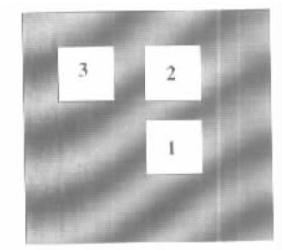
Figure 3 Schematic diagram of the position where the chip is pasted on the substrate
The test procedure is as follows: the pad corresponding to the resistor to be tested on the silicon wafer is first connected to the pin of the substrate by gold ball bonding, and the resistance value under the condition of no stress is measured; when the substrate is heated to 60 ° C, the bonding is performed. The agent was filled between the substrate material and the chip and then cured in an oven at 150 °C. The curing process is carried out in accordance with the instructions for use of commercial products, and the change in resistance with temperature is measured during the curing of the organic binder. After the adhesive is fully cured, the final resistance value is measured again. The heat treatment was carried out 24 hours after the completion of the curing. Taking into account the special relationship between the curing temperature and the adhesive, the heat treatment after curing still uses the curing system, that is, the cured sample is re-raised in the oven to a curing temperature of 150 ° C, then naturally cooled, and then the resistance value is recorded again. .
The binder parameters selected are: glass transition temperature θg = 135OC, low temperature thermal expansion coefficient α1 ( < θg) = 28 X 10 - 6 / °C, high temperature thermal expansion coefficient α2 ( > θg) = 90 X 10 - 6 / °C, The modulus of elasticity is E = 9 Gpa, the bond strength is 145 Mpa, and the cure regime is 150 OC X 60 min. The FR4 material used in the experiment has a coefficient of thermal expansion of 16 X 10 - 6 /° C. and a Si of 3. 2 X 10 - 6 / ° C.