Serial RapidIO improves modular base station design
The modular design and manufacture of cellular base stations are critical to combining 3G mobile services such as video, voice, and data, commonly known as "triple services." But why is modular design so important?
In fact, customers believe that base station prices must fall by 80% each year. In order to provide services with high bandwidth requirements as cost-effectively as possible, service providers also require a significant increase in throughput—guaranteed 10 Gbps. This leads to the question of how to solve the obvious contradiction of reducing costs and improving performance?
In the future, modularity will definitely reduce manufacturing costs and equipment upgrade costs to meet more stringent requirements. However, with the deployment of standard application-specific system components (ASSC), modularity can also meet significantly increased system performance requirements. What is the result? Higher throughput can increase the service capacity of any given time slot, which can reduce the unit cost of service.
So, how do we achieve modularity? There is still a long way to go to achieve this goal by using lower cost standard components to replace relatively expensive cellular and FPGA-based ASIC devices. However, if these standard components interoperate without using a custom-designed interface, a standard interface is required. Custom-designed interfaces are the natural enemies of the efficient use of standard components and can hinder manufacturers from maximizing the ability to use modularity.
Serial RapidIO is an open standard interface designed to solve this problem in embedded systems. On the implementation board
This article will introduce how the use of two serial RapidIO ASSCs in modular 3G base station design can improve performance by 20%, and according to the base station designer, how to reduce material costs by 50% to 75% compared to other solutions (BOM). In particular, we describe a standard ASSC—10 Gbps serial buffer, which can eliminate the severe throughput bottleneck of the base station—the bottleneck of frame samples; at the same time, we also discussed how to use another standard ASSC, which is preprocessing exchange. By reducing the load on the digital signal processor (DSP) to improve system performance.
Frame sample comparison bottleneck
Today's wireless base stations must process the same set of data multiple times to decode different information. For example, in the 3G system, the same hardware module (DSP or chip rate processing ASIC) needs to obtain 10 ms of sample frame data to first perform random access channel (RACH) decoding, and then perform data channel (DCH), and the same data Must be accessed by all DSPs in the cluster.
However, interference from the radio frequency (RF) environment can cause data distortion, destruction, and data packet loss. To this end, the base station must compare the data in the time domain to improve the efficiency of the real-time processing algorithm program to compensate for these errors and losses. The base station needs to compare the previous frame sample (n-1) with the current frame sample (n) . However, in higher data throughput systems such as 3G base stations, the samples are quite large, and the system throughput will be limited by performing such large sample comparisons.
The frame sample comparison problem usually consumes valuable system resources to achieve the required speed, and limits the base station system's ability to support value-added services at a competitive price. The next-generation wireless infrastructure of 3G, 4G and above requires a base station data processing speed of 10 Gbps to maximize the number of transmissions to independent terminals.
Several methods that are feasible but not ideal
Limited local storage capacity is the bottleneck. Basically, the DSP local memory does not have enough capacity to perform this comparison in one operation. One way to solve this problem is to divide the big data sample into several fragments for separate processing, and then integrate these results. However, this affects baseband throughput and reduces performance. In any case, these local memories should be dedicated to cache and program code. If they are used for other purposes, it will lead to the need for more memory elsewhere on the board, while also causing device and space costs and memory management issues. Of course, base station manufacturers can partially compensate for the decline in performance by increasing the number of DSPs or increasing the speed. However, this incremental approach does not solve the fundamental problem-storing a large number of data samples and quickly passing them to the DSP for processing.
Since storage capacity is a challenge we face, we can add a local memory on the board as a buffer to feed other local memories. This will complicate storage management, but it is only an expedient measure to alleviate the bottleneck problem, but not to solve this problem.
Another option is that we can use replicated parallel memory. However, this will make the device and board space very expensive and will significantly increase the BOM. In addition, as throughput requirements increase, circuit boards need to be redesigned to accommodate larger memories. Therefore, this solution is not easy to expand.
Another method is to use FPGA to connect the baseband switch to store data in the shared system memory, which is a custom design with high design cost, higher risk and higher BOM. In addition, the use of standard devices with standard interface specifications for custom devices can disrupt the main startup procedure of the module. The basic architectural method to solve this problem is to make the data parallel. However, this will significantly increase the input and output of the device. In addition, it obviously needs to occupy more circuit board area and may potentially reduce the number of channels supported by a given circuit board. The end result is a substantial increase in BOM and service delivery unit costs.
Finally, all these pure storage solutions do not introduce intelligent system data processing. Therefore, the customized circuit must be able to find the missing data packets, and at the same time use virtual packets to fill the gaps, thereby maintaining packet synchronization. A standard sample comparison solution that integrates the required intelligence can serve two purposes.
Appropriate solution
Based on the evaluation and analysis of some of the above solutions, we list the performance of an optimal solution as follows:
â— The solution must include a memory with sufficient capacity to store a large number of data samples.
â— In order to "verify" the design in the future, the memory must be expandable.
â— There must be a serial interface between the memory and the DSP cluster to minimize the number of I / O.
â— The serial interface of the memory must be fast enough to feed the DSP with 10 Gbps board-level throughput.
â— The serial interface must meet the industry standard specifications adopted by DSP manufacturers.
â— Devices must use intelligent data processing to eliminate the need for specialized devices that must be custom designed.
â— The device must eliminate any and all custom methods-must be standard application-specific system components.
In other words, the solution is a
The serial buffer activated by Serial RapidIO has a capacity of 18MB and can be expanded to 90MB by an optional quadruple data rate (QDR) method, which helps to achieve real-time comparison of large, continuous frame samples at 10 Gbps.
The 10 Gbps performance and high storage capacity can ensure that the DSP uses base station applications to perform full-frame calculations in real time with approximately 15 ms of data in one execution. This device requires only 16 I / O pins, which not only minimizes the number of I / Os, but also enables direct connection to the FPGA.
The serial buffer contains intelligent monitoring and control circuits that can automatically identify and compensate for lost data packets to maintain data synchronization. In addition, it can also be used as a master node to determine when and where to send data, and start data transmission without other DSP assistance.
Improve digital processing throughput
Solved the sample comparison problem, we can look at another aspect of using Serial RapidIO ASSC, namely the processing performance itself. Of course, increasing the number and / or performance of DSPs will increase system throughput. However, the throughput can be simply increased by making the DSP load optimal. This is the role of the preprocessing switch chip.
The preprocessing switch chip is located between the RF backplane and the DSP, and intercepts the data before it reaches the DSP. The switch chip helps to carry out packet processing on the payload data and optimize the payload before the DSP performs wireless operations. The device can preprocess data while exchanging information packets. Then the output packet will be transmitted to the DSP cluster by multicast. This pre-processing device can not only provide the pre-processing function, but also can determine the "programmable at any time" modification of the DSP configuration software based on the bandwidth, flow and call data. Therefore, this switching chip allows the system to dynamically adjust, start, and close paths to meet the needs of changing bandwidth. Unlike previous wireless base station architectures, this pre-processing chip provides inherent scalability that can be well utilized in the future.
This switching chip can be customized to suit cellular-based chips or FPGAs. However, this application is ideal for standard devices using standard interface specifications. A large number of ASSC tests show that it can reduce the DSP load by 20%, thereby effectively improving the DSP's capabilities. In addition, replacing old-fashioned FPGAs and dual-port memories can reduce cost and design complexity.
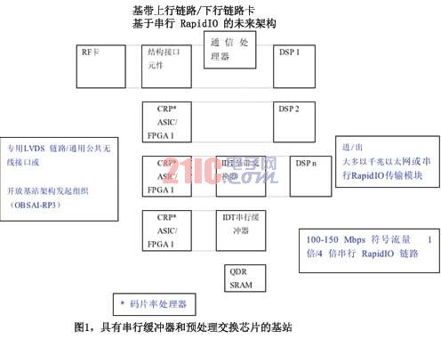
Development of base stations with serial buffers and preprocessing switching chips
Base station designers say that the combination of serial buffers and pre-processing switching chips not only reduces DSP load by 20%, but also reduces material costs by 50% to 75% compared to other solutions. Please refer to Figure 1 for the base station circuit board using a combination of two devices.
Obviously, the prerequisite for successful design is that these two ASSC combinations work seamlessly with the DSP. To achieve such operations, base station designers can use a development platform jointly developed by major component manufacturers. Based on such a platform, software programming and early prototypes can be started to accelerate time to market. The development platform includes 4 ultra-high performance DSPs with switching connections, pre-processing switching chips, and daughter card expansion ports that support other serial RapidIO endpoints including serial buffers. It also includes all the software needed to speed up installation, initialization, and on-site case execution. The platform has 3 Gigabit Ethernet backplanes, 1 line I / O; each DSP has up to 128 MB of DRAM DDR2; flash memory (serial high speed) and I2C; system main boot JTAG, MMC; used for other Applied IPMI MMC control; and 1 independent operation of local power selection.
to sum up
Modular design requires the use of standard components with standard interfaces. The serial buffer can solve the problem of frame sample comparison, and the preprocessing switching chip can solve the throughput-intensive data processing and switching problem. The combination of serial RapidIO can provide users with complete processing and storage solutions, helping them cost-effectively provide advanced DSP-intensive wireless services such as video, voice and data to end customers. In addition, it can solve the increasing throughput limitations of wireless infrastructure; compared with other solutions, it can reduce DSP load by 20% and reduce material costs by 50% to 75%.
Guangzhou Ehang Electronic Co., Ltd. , https://www.ehangmobile.com