The sensor network represents the convergence of information acquisition (sensing), transmission, and processing technologies. In certain scenarios, communication cannot depend on pre-configured infrastructure, but instead requires mobile communication solutions that can dynamically establish a temporary network. As a result, sensor networks are expected to usher humanity into an era where sensing and networking are seamlessly integrated.
At the heart of any RF receiver is the low noise amplifier (LNA), which plays a critical role in determining the overall system performance. Since it is the first stage connected directly to the antenna, its noise characteristics significantly impact the signal quality. Additionally, the received signal is often weak, so the LNA must provide sufficient gain to amplify the signal without introducing excessive noise.
This paper presents a low noise amplifier operating at 2.4 GHz, designed using the SM IC 0.13μm RF CMOS process. Power consumption is a primary concern for wireless sensor nodes, making it essential for the amplifier to balance gain, noise figure, bandwidth, linearity, and stability while keeping power usage within limits. However, achieving both minimal noise and maximum gain simultaneously is challenging. Thus, optimizing input and output matching while maintaining low noise under constrained power becomes a key design challenge.
The circuit structure of the LNA is based on a cascode differential configuration. This design helps reduce the Miller effect and improves reverse isolation by lowering the input impedance. The use of on-chip resistors and inductors ensures proper impedance matching at both the input and output stages, enhancing the amplifier’s stability and performance.
The gate length of the MOS transistors is set to the minimum process value of 0.13 μm to minimize noise. By adjusting the gate widths, the transconductance of the transistors can be fine-tuned to optimize gain. The design operates at 1.2 V, with a DC bias voltage set to ensure sufficient linearity and stable operation.
A gain control circuit is implemented using MOS transistors controlled by external voltages. Adjusting the current through these transistors allows for dynamic gain control, enabling the amplifier to adapt to varying signal conditions.
For input matching, the small-signal model of the amplifier is analyzed to ensure optimal impedance matching. Additional capacitors and inductors are used to tune the input impedance, ensuring maximum signal transfer efficiency and minimizing reflection. This careful design approach contributes to the overall performance and reliability of the low noise amplifier in wireless sensor network applications.
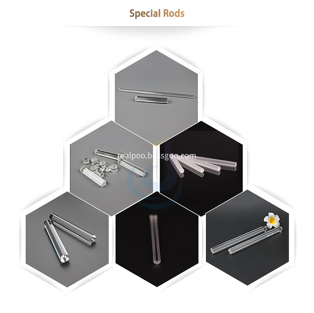
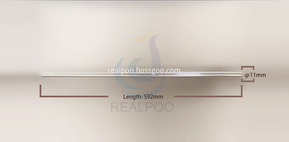
Realpoo Optics' Guide Rods are single straight rods which suit applications requiring bulk light transmission as well as optical mixing in straight shapes. They are typically used to isolate or remotely locate photo sensors and light sources.
About polishing, we can offer different options: Flat surface polishing and bent surface not polishing; or bent surface polishing and two flat surfaces not polishing ; or all surfaces not polishing. All is depending your requirements.


Glass Rod,Collimating Lens,Optics For Lasers,Glass Cylinder
Changchun Realpoo Photoelectric Co., Ltd. , https://www.optics-realpoo.com