In recent years, software-defined radio (SDR) has experienced rapid development and has demonstrated its advantages in various fields. This paper focuses on the implementation of digital audio broadcasting (DAB) baseband signal processing using software radio technology, which demands high-speed real-time digital signal processing and transmission capabilities from the software radio platform. High-speed programmable logic devices such as FPGAs, along with a rich library of IP cores, provide an ideal platform for efficiently implementing SDR systems.
**1 PCIe Bus Demonstration**
PCIe is the third-generation I/O bus interconnect technology and has become the leading standard for personal computers and industrial equipment. Compared to the traditional parallel PCI bus, PCIe uses a serial, point-to-point connection, offering higher data transfer rates and better scalability. For example, the 8-channel PCIe 2.0 hard core used in this paper can achieve a theoretical transfer rate of 4 GB/s [1], and the bus width can be configured as ×1, ×2, ×4, or ×8 channels depending on the requirements. In comparison with other serial interfaces like RapidIO and HyperTransport, PCIe offers superior performance and greater flexibility [2].
**1.1 PCIe Bus Implementation**
Currently, there are two main approaches to implementing the PCIe bus: dedicated interface chips (ASICs) and FPGA-based solutions. The first approach typically combines ASICs with FPGAs or DSPs. Dedicated PCIe interface chips, such as the PEX8311, simplify the user's interaction with the PCIe protocol, reducing development complexity. However, this method results in a more complex hardware design, limited functionality, and poor flexibility and scalability.
The second approach utilizes IP cores to implement the PCIe protocol, allowing users to develop custom functions and drivers, providing greater programmability and reconfigurability. Additionally, using a single-chip FPGA reduces cost and circuit complexity, making it more compatible with system-on-a-chip (SoC) design concepts. This paper employs the Xilinx Virtex-6 FPGA and its integrated PCIe block to implement a high-speed PCIe interface in double-buffer mode.
**1.2 Double Buffer vs. Single Buffer Comparison**
Let’s take a write operation (data transfer from FPGA to memory) as an example. The block diagram of the double-buffered PCIe system is shown in Figure 1. For simplicity, we refer to the FPGA-based system as SRSE (Software Radio System with PCIe).
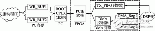
*Figure 1: Double-buffered PCIe system block diagram*
The PC-side driver allocates two buffers (WR_BUF1 and WR_BUF2) in system memory for data storage. The addresses of these buffers are stored in the DMA registers (DMA_Reg1 and DMA_Reg2) on the FPGA side. The Root Complex connects the CPU, memory, and PCIe devices, and acts as the central controller that generates transfer requests [3]. The PCIe core, provided by Xilinx, handles the PCIe protocol. The DMA engine facilitates data transfer between the DSP core and the PCIe device. The DSP core represents user-designed algorithms or applications.
For instance, the DSP core writes data into the TX_FIFO. The DMA engine sends this data to the PCIe core in the form of Transport Layer Packets (TLPs), where the packet headers are sourced from the register DMA_Reg1. When SRSE writes data to WR_BUF1, the driver allocates another buffer, WR_BUF2, and updates the address information in DMA_Reg2. Once the DMA engine triggers an MSI interrupt for WR_BUF1, it switches the header information to DMA_Reg2. The driver then switches to WR_BUF2 to continue the data transfer.
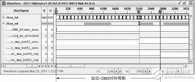
*Figure 2: PCIe bus interrupt delay measurement*
In contrast, the single-buffer mode operates differently. During a write operation, the driver allocates one buffer (WR_BUF) each time, storing its address in the DMA register (DMA_Reg). When WR_BUF is full, the DMA engine generates an MSI interrupt and notifies the driver through the PCIe core. The driver then allocates a new buffer and updates the DMA register via the PCIe bus. This process introduces a delay due to interrupt handling and DMA register updates, requiring a larger TX_FIFO to prevent data loss during this period.
To accurately measure the interrupt delay, a platform based on a DELL T3400 PC and ML605 development kit was built. The ChipScope waveform results, shown in Figure 2, indicate that the DMA interrupt occurs at time 0 (mwr_done: 0 → 1). The PCIe core then issues an MSI interrupt to the driver, which checks the interrupt register at time 2241 (irq_wr_accessed: 1 → 0). The driver allocates a new buffer and updates the DMA register at time 2802 (wr_dma_buff0_rdy: 0 → 1). During these 2802 clock cycles, the PCIe device could not write data to memory. With a 250 MHz clock frequency, the interrupt delay is T = 2802 × (1/250 MHz) = 11.2 μs. Assuming the DSP core generates data at 200 MB/s, approximately 2241 B of data would be generated during the delay. Considering other unpredictable factors, such as interrupt blocking, the TX_FIFO must have several kilobytes of space to avoid data loss. This presents a significant challenge for limited hardware resources like Block RAM in FPGAs.
Compared to the single-buffer mode, the double-buffer mode offers several advantages:
1. Updating buffers does not introduce interrupt latency, allowing smaller FIFOs to meet requirements and saving hardware resources.
2. The double-buffer mode extends the time the driver has to handle interrupts, simplifying buffer data processing and significantly reducing the packet loss rate.
3. Data transmission and processing of memory buffers can occur in parallel, ensuring the system’s real-time performance.
4. Double buffering is more suitable for Scatter/Gather DMA, replacing block DMA to improve memory efficiency.
High Voltage Lan Transformer,High Voltage Pwoer Pulse Transformer,Cmc Coilfor Automotive Product,High Voltage Pulse Transformer
IHUA INDUSTRIES CO.,LTD. , https://www.ihuagroup.com