An embedded system is an application in which embedded software is embedded in the hardware of a computing device. We are now surrounded by embedded systems that bring convenience and luxury to our lives, including mobile handsets, washing machines, microwave ovens, ATMs, air conditioners and more. Due to certain application requirements, engineers must perform embedded designs in specific ways that differ from other design types.
The following is a brief overview of the steps to design an embedded system:
1. Recommendation: An innovative concept or system that makes life easier and/or reduces the manpower required to complete a task.
2. Definition: The next step is to design the entire system, including the performance of the system under various possible input conditions. The definition may be the most critical part, because any mistakes in the definition phase will affect the work of the entire system.
I. Input/Output Considerations: Define what the system output will be at a particular input, considering the system as a black box;
II. Mathematical Modeling: An algorithm designed to let the system work on demand;
III. Functional Modeling: The ability of the design system to accept input and generate the desired output.
3. Technology Choice: Based on the above points, designers can evaluate available technologies, select which devices meet all requirements, and balance efficiency, cost, and time-to-market.
4. Integration and PCB Design: List all the components needed to implement the features you want and design their layout on the PCB. Wiring and all other paths must minimize electromagnetic interference (EMI) and should avoid errors. When designing the PCB, pay special attention to the floor and all components that are grounded on the PCB.
5. Firmware development and debugging: Since the hardware needs instructions to execute in the way we want, we need to write code for each component used by the hardware. This is exactly what the firmware (ie application code) does. Firmware should minimize complexity. In addition, we may encounter many errors and failures when writing code, which requires an appropriate debugging protocol.
6. Testing: The test code part is required for debugging, and during the testing process, we need to detect the entire system, that is, the hardware and the software that drives the hardware.
7. Documentation: Anyone who browses your complete application design should not ask you "What does this mean?" "How does this work?" To avoid being bothered by such problems, we should be prepared for complete and complete documentation.
Problems in the current design process:
When developing embedded applications, we should fully understand the different chips and their functions and complex architecture, and then create the system design flow. Next, we need an application to provide functionality for our products and components, for which we have to write code. When writing code, system requirements are constantly changing, and designers need tools to support different debugging protocols. We may not be able to reuse the code, we want to integrate multiple features in a single system. In view of the above problems, embedded system design needs to consider various issues such as overall system price, performance, acceleration of product launch process, size, power consumption, maintainability, security, and memory capacity. In addition, developers of embedded systems want to implement programmable analog and digital peripherals on a single chip. Therefore, the development of a system-on-a-chip (SOC) is quite cumbersome for developers.
Embedded systems are becoming more complex and require programmability in almost any situation. To do this, designers need tools to deal with this difficult situation while providing a user-friendly environment to develop applications. Although we have some market for SOC tools, we don't fully understand the capabilities of these tools. In addition, tools must be able to maximize the product's characteristic potential. To illustrate this, let's take an example of a complex architecture chip that integrates almost all analog and digital programmable peripherals on a single chip. We may find that reading and understanding the relevant configuration registers and other underlying information related to the device can be complicated, so we need an intuitive and easy-to-use system design tool to hide the underlying information, making it easier for us to focus on the system. application.
In short, we need a tool that not only speeds up the time-to-market, handles all development considerations intuitively and efficiently, but also costs too much, and supports projects between different chips depending on the requirements. Transplantation.
PSoC Creator:
Programmable System-on-Chip (PSoC) manufacturers have come to realize that developers need to have a complete system on a single chip, with both analog and digital functions, and that analog and digital functions should be fully programmable. To develop embedded applications that work on these chips and to provide solutions to all of these issues, Cypress Semiconductor has introduced PSoC Creator. PSoC Creator's unique schematic-based format allows designers to develop applications without having to manually manage the architecture or configuration registers. Now, all we have to do is think about the design and then draw the design by dragging and dropping components from the Cypress component library or our own component library into the design schematic. This is like drawing a system block diagram, regardless of what device is being used. It is because of the revolutionary graphic design editor that supports a unique and powerful hardware and software co-design environment that we can achieve. Please note that this tool not only combines the software development environment and the intuitive graphical design editor, but also supports real-time testing of new concepts, quickly responding to hardware changes, creating a library of sharable design components, and providing customization. Peripherals support error-free interaction of on-chip peripherals and enable complete design with built-in debugger.
In short, the function and use of the tool can be divided into 4 steps as shown below:
Step 1: Design and configure the drag and drop component to connect the peripheral I/O to the pin to set the clock frequency
Step 2: Develop calls to the built-in API C / assembly language programming is more error-free and more convenient
Step 3: Debug the built-in debugger to see the type, address, and value of any variable at runtime View the stack, memory, and registers at runtime
Step 4: Reuse quickly and easily to create future designs Integrate work design into reusable components
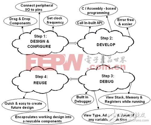
Figure 1. Steps to create a project with PSoC Creator
PSoC Creator combines a C-based development process with an automatically generated component API in your design. It seamlessly migrates between devices (such as 8-bit to 32-bit) based on changes required in subsequent phases. Even if you want to migrate between different device families, we don't need to worry about memory mapping, mnemonics, and so on. A unique advantage here is that the design process does not have to worry about the family of target chips, because the designer can change the device at any time during the development cycle without having to modify anything in the project.
Now let's take a look at a project example to better understand the functionality and usability of PSoC Creator to develop embedded applications in real-world environments. This project example demonstrates how to control the brightness of an LED by using pulse width modulation (PWM).
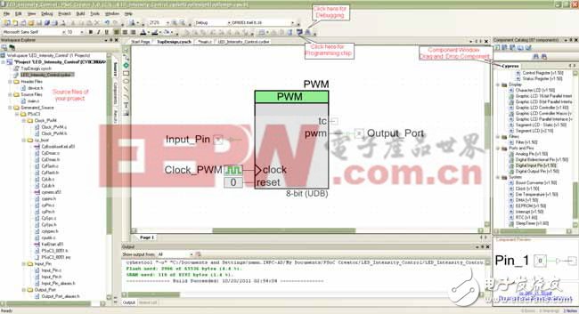
Figure 2: Schematic of PSoC Creator
Switching Current Transformer,Outdoor Switching Current Transformer,Busbar Built-In Current Transformer,Outdoor Split Core Current Transformer
Zibo Tongyue Electronics Co., Ltd , https://www.tongyueelectron.com