1) Introduction to CH451
CH451 can be used in LED digital tube display driver, keyboard scanning control, μP monitoring circuit and other fields. The chip package includes dual in-line DIP28, SOP28 and DIP24S packages. Its built-in RC oscillator circuit can directly drive 8-bit digital tube or 64-bit LED directly, with BCD decoding or non-decoding function, which can realize left shift, right shift, left loop, right loop, independent flashing of each digit, etc. control function. The CH451 has a built-in high-current drive stage with a segment current of no less than 30 m A, a word current of no less than 160 mA, and 16 levels of brightness control. The device has a built-in 64-key keyboard controller, which can realize 8×8 matrix keyboard scanning and built-in debounce circuit, which can provide functions such as button interrupt and button release flag. The CH451 can be selected from a simple 1-wire serial interface or a high-speed 4-wire serial interface, and has a built-in power-on reset that provides both an active-high reset and an active-low reset, as well as a built-in watchdog circuit. A multi-function peripheral chip that integrates digital tube display driver and keyboard scan control and μP monitoring. With CH45l extended keyboard display interface, it has the advantages of simple interface, less CPU resources, simple peripheral devices, high cost performance, etc. It can be widely used in various single-chip systems.
2) Introduction to CH451 operation commands
CH451 has 11 operation commands, each operation command is 12 bits, of which the upper 4 bits are identification codes, the lower 8 bits are parameters, and x can be any value (the same below)
Empty operation (0000xxxxxxxxB)
The null operation command has no effect on the CH451. The command can send an operation command to the subsequent stage cH451 through the preceding stage CH451 in multiple CH451 cascade applications without affecting the state of the previous stage cH451. For example, to send the operation command 001000000001B to the subsequent stage CH45l in the two-stage cascade circuit (the DIN pin of the latter stage CH451 is connected to the DOUT pin of the previous stage CH451), as long as the empty operation command 000000000000B is added after the operation command. Send, then, the operation command will pass the pre-stage cH451 to the subsequent stage cH451, and the null operation command is left to the pre-stage CH451. In addition, in order to change DCLK to clear the watchdog timer without affecting CH451, a null operation command can also be sent. In non-cascading applications, the no-op command can only send the upper 4 bits.
Chip internal reset (001000000001B)
The internal reset command resets the various registers and various parameters of the CH451 to their default state. When the chip is powered on, CH45l is reset. At this time, each register is reset to 0, and various parameters are restored to the default values.
Word data shifts left (001100000000B)
The word data left shift command shifts the word data of CH451 to the left one time, that is, moves one bit from DIGO to DIG7, and then the rightmost DIG0 fills in data 00H. For example, when the digital tube DIG7 to I) IGO displays "87654321", the word data left shift command is executed, and the display changes to "765432l" (no decoding method) or "76543210" (BCD decoding method).
Word data is shifted to the right (001100000010B)
The word data right shift command shifts the word data of cH45l to the right, that is, moves one bit from DIG7 to DIGO, and then the leftmost DIG7 adds data 00H. For example, when the digital tubes DIG7 to DIGO display "8" 7653321", the word data right shift command is executed, and the display is changed to "8765432" (no decoding method) or "08765432" (BCD decoding method).
Word data left loop (001100000001B)
The word data left loop command loops the word data of CH451 to the left one time, that is, moves one bit from DIGO to DIG7, and then the rightmost DIGO fills in the data of the original DIG7. For example, when the digital tube DIG7-DIGO displays "8" 765432l", the word data left loop command is executed, and the display changes to "76543218".
Word data right loop (001100000011B)
The word data right loop command loops the word data of CH451 right once, that is, moves one bit from DIG7 to DIGO, and then the leftmost DIG7 fills in the data of the original DIG0. For example, when the digital tube DIG7-DIGO displays "8765432l", the word data right loop command is executed, and the display changes to "18765432".
Set system parameters (010000000WDOG][KEYB][DIsP]B)
This command is used to set the system level parameters of cH451, such as watchdog enable wDOG, keyboard scan enable KEYB, display driver enable DISP. Each parameter can be controlled by 1-bit data, and the corresponding data position is set to 1 to enable the function, otherwise the function is turned off (default value).
Set display parameters (0101[MoDE][LIMIT][INTENSITY]B)
This command is used to set the display parameters of CH45l, such as decoding mode MODE (1 bit), scan limit LIMIT (3 bits), display brightness INTENSITY (4 bits) and so on. When the decoding mode MODE is 1, the BcD decoding mode is selected, and when it is 0, the non-decoding mode is selected. The CH451 defaults to the non-decoding mode. At this time, the 7-bit 0 of the byte data in the 8 data registers respectively correspond to the decimal point of 8 digital tubes and the segment G to the segment A. When the data bit is 1, the corresponding data The segment (or LED) is lit; when the data bit is 0, it is off. The cH451 works in the BcD decoding mode and is mainly applied to the digital tube driver. As long as the single-chip microcomputer gives the BcD code of the binary number, it can be decoded by the CH451 and directly drives the digital tube to display the corresponding character. The BcD decoding mode is to perform BcD decoding on the bit 4 to bit 0 of the byte data in the data register, and can be used to control the output of the segment driving pins SEG6 to SEGO, which correspond to the segment G-segment A of the digital tube. At the same time, the bit 7 control segment of the byte data can be used to drive the output of the pin SEG7 to correspond to the decimal point of the nixie tube. Bits 6 and 5 of the byte data do not affect the output of the BcD decoding, and they can be any value. BCD decoding of bit 4 to bit 0 can display the following 28 characters, of which 00000B-01111B respectively correspond to "0~F", and 10000B-11010B respectively correspond to "" space, "+", + or plus sign, " One or minus sign, "=" equal sign, "left bracket", "right bracket", "one" underline, "H", "L", "P", "." decimal point, the rest are spaces .
The scan limit uMIT control bits 00lB to 1l1B and 000B (default values) can set the scan limits 1 to 7 and 8, respectively. The 0001B to 1111B and 0000B (default values) of the display brightness INTENSITY control bits are used to set the display drive duty ratios 1/16 to 15/16 and 16/16, respectively, to achieve 16-level display brightness control.
Set the flicker control (0110[D7s1][D6S][D5s][D4S][D3S][D2S][D1S][D0S]B)
The setting flicker control command is used to set the flashing display attribute of CH451, where D7s-130S correspond to 8 words driving DIG7~DIGO respectively. The flashing attribute D7s-DOS is controlled by 1-bit data respectively, and the corresponding data position is set to 1 to enable flashing display, otherwise it is normal display, not flashing (default value).
Load word data (1[DIG-ADDR]DIG_DATAlB)
The Load Word Data command is used to write the byte data DIG_DATA (8 bits) to the data register specified by DIG_ADDR (3 bits). The 000B-111B of DIG_ADDR is used to specify the address O~7 of the data register, and corresponds to the 8 digital tubes driven by the DIGO-DIG7 pin. DIG_DATA is the byte data to be written.
Read button code (0111xxxxxxxxB)
The Read Key Code command is used to obtain the key code of the valid key detected by the cH451. This command is the only command with data return. CH451 usually outputs the key code from the DOUT pin. The key code is always 7-bit data, the highest bit is the status code, and the bit 5~bit O is the scan code. The bit data B7-B0 of the read key code command may be an arbitrary value, so the controller can shorten the operation command to the 4-bit data B1 to B8. For example, when the CH451 detects a valid button and interrupts, if the button code is 5EH, it first issues a read button code command 011lB to the CH451, and then obtains the button code 5EH from DOUT.
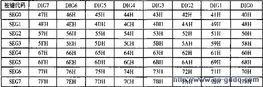
The key code provided by CH451 is 7 bits. Bit 2 is a column scan code, bits 5 to 3 are line scan codes, and bit 6 is a status code (key is pressed to 1, and key is released as O). For example, when the button connecting DIG3 and SEG4 is pressed, the button code is 63H, and after the button is released, the button code is 23H. The MCU can read the key code at any time, but generally reads the key code when the CH451 detects a valid key and generates a keyboard interrupt. At this time, the bit 6 of the key code is always 1. In addition, if you need to know when the button is released, the MCU can periodically read the button code by querying until the bit 6 of the button code is 0. Table 1 is the key code provided by CH451 when the key connected between DIG7-DIGO and SEG7-SEGO is pressed. These key codes have a certain rule. If the key code when the key is released is required, the bit 6 of the key code in Table 2 can be set to 0, or the key code in the table can be subtracted by 40H. It should be noted that the CH451 does not support key combinations, that is, two or more keys cannot be pressed at the same time.
Table 1 CH451 button code
3) Hardware connection
The CH451 can drive 8-bit digital tubes at one time and communicate serially with the microcontroller. Support digital tube left shift, right shift, left loop, right loop, independent flashing, 16 levels of brightness control and other functions. It is a powerful assistant for controlling multiple digital tubes by MCU. Now MEGA16 MCU (MEGA16 is AVR MCU, modified program can be applied to 8051 MCU, PIC MCU, MSP430 MCU) to drive the program of CH451, hope to be useful. Details of the CH451 can be downloaded from the official website. Figure 1 is a hardware connection circuit diagram.
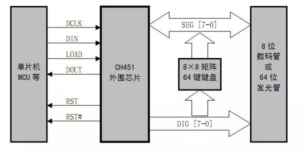
Figure 1: CH451 and LED digital tube connection circuit diagram
4) Program examples
AVRCH451 driver header file
#ifndef_CH451_H
#define_CH451_H
#include
//CH451 command macro definition
#defineCH451_RESET0x0201//Reset
#defineCH451_LEFT MOV 0x0300//Set the movement mode - Shift left
#defineCH451_LEFTCYC0x0301//Set the mobile mode - left
#defineCH451_RIGHT MOV 0x0302//Set the movement mode - right shift
#defineCH451_RIGHTCYC0x0303//Set the mobile mode - right
#defineCH451_SYSOFF0x0400//Off display, keyboard, watchdog
#defineCH451_SYSON10x0401//Open display
#defineCH451_SYSON20x0403//Open display, keyboard
#defineCH451_SYSON30x0407//Open display, keyboard, watchdog function
#defineCH451_DSP0x0500//Set the default display mode
#defineCH451_BCD0x0580//Set BCD decoding mode
#defineCH451_TWINKLE0x0600//Set the flicker control
#defineCH451_KEY0x0700//Read the keyboard code
#defineCH451_DIG00x0800//Digital tube position 0 display
#defineCH451_DIG10x0900//Digital tube position 1 display
#defineCH451_DIG20x0A00//Digital tube position 2 display
#defineCH451_DIG30x0B00//digital tube position 3 display
#defineCH451_DIG40x0C00//digital tube position 4 display
#defineCH451_DIG50x0D00// Digital Tube Position 5 Display
#defineCH451_DIG60x0E00//digital tube position 6 display
#defineCH451_DIG70x0F00//digital tube position 7 display
//Port macro definition
#defineDCLK(1<<;PA3)
#defineDIN(1<<;PA5)
#defineLOAD(1<<;PA7)
#defineDOUT(1<<;PE5)
#defineCH451_DCLK_HIGHPORTA|=DCLK//clock signal
#defineCH451_DCLK_LOWPORTA&=~DCLK
#defineCH451_DIN_HIGHPORTA|=DIN//Data Input
#defineCH451_DIN_LOWPORTA&=~DIN
#defineCH451_LOAD_HIGHPORTA|=LOAD//Command load signal, rise delay activation
#defineCH451_LOAD_LOWPORTA&=~LOAD
#defineCH451_DOUTPINE&DOUT//Keyboard Interrupt and Key Value Data Output
externucharKeyValue; / / key value global declaration
/ / Function declaration
voidCH451_WriteCommand(uintCommand);//CH451 write command function
voidCH451_Init();//CH451 initialization function
voidCH451_GetKeyValue();//CH451 keyboard code reading function
voidCH451_DisplayDig(ucharDIG, ucharData, ucharPoint); / / CH451 display a digital tube function
#endif
AVR CH451 driver file
#include"CH451.h"
ucharKeyValue; / / key value
/ / Yin digital tube coding table
constucharDSYCode[18]={0x3F,0x06,0x5B,0x4F,//0,1,2,3
0x66, 0x6D, 0x7D, 0x07, / / ​​4, 5, 6, 7
0x7F, 0x6F, 0x77, 0x7C, / / ​​8, 9, A, b
0x39, 0x5E, 0x79, 0x71, / / ​​C, d, E, F
0x40, 0x00}; / / -, all out
constuintDigCode[8]={CH451_DIG0, CH451_DIG1, ​​CH451_DIG2, CH451_DIG3,
CH451_DIG4, CH451_DIG5, CH451_DIG6, CH451_DIG7};
/ / keyboard code table
constucharKeyCode[16]={0x40,0x41,0x42,0x43,//0,1,2,3
0x48, 0x49, 0x4A, 0x4B, / / ​​4, 5, 6, 7
0x50, 0x51, 0x52, 0x53, / / ​​8, 9, A, B
0x58, 0x59, 0x5A, 0x5B}; / / C, D, E, F
//CH451 write command function
voidCH451_WriteCommand(uintCommand){
Uchari
CH451_LOAD_LOW; / / command begins
For(i=0;i<12;i++){//feed 12-bit data, low in front
If(Command&0x0001)CH451_DIN_HIGH;//output low data
elseCH451_DIN_LOW;
CH451_DCLK_LOW;
Command>>=1;//The data is shifted to the right by one
CH451_DCLK_HIGH; / / rising edge is valid
}
CH451_LOAD_HIGH; / / load data
}
//CH451 initialization function
voidCH451_Init(){
CH451_DIN_LOW; / / low enable serial interface
CH451_DIN_HIGH;
CH451_WriteCommand(CH451_RESET);//Reset CH451
CH451_WriteCommand(CH451_SYSON2);//Open display, keyboard
DDRE&=~DOUT;//PE5 input direction
EICRB|=(1< EIMSK|=(1< } //CH451 key value reading function voidCH451_GetKeyValue(){ Uchari ucharGetKeyValue=0x00;//keyboard code CH451_WriteCommand(CH451_KEY);//Send read key value command For(i=0;i<7;i++){ GetKeyValue<<=1; If(CH451_DOUT)GetKeyValue|=1;//Read the data of 451 from high to low elseGetKeyValue|=0; CH451_DCLK_LOW; / / falling edge is valid CH451_DCLK_HIGH; } If(GetKeyValue==0x00)return;//Read key code is 0 skip For(i=0;i<16;i++){//Find the key value corresponding to the keyboard code If(GetKeyValue==KeyCode){ KeyValue=i; Break; } } } //CH451 displays a digital tube, DIG selects the digital tube, the number to be displayed by Data, and whether Point displays the decimal point. voidCH451_DisplayDig(ucharDIG,ucharData,ucharPoint){ If(Point==1)CH451_WriteCommand(DigCode[DIG]|(DSYCode[Data]|0x80)); elseCH451_WriteCommand(DigCode[DIG]|DSYCode[Data]); } Mining is the process of creating a block of transactions to be added to the Ethereum blockchain in Ethereum's now-deprecated proof-of-work architecture.
Mining is the lifeblood of any proof-of-work blockchain. Ethereum miners - computers running software - used their time and computation power to process transactions and produce blocks prior to the transition to proof-of-stake.
ETH Miner:Antminer E9 2.4Gh/S,Bitmain E9 2.4Gh/S,Bitmain Antminer E9 2.4Gh/S
Eth Miner ,Antminer E9 2.4Gh/S,Bitmain E9 2.4Gh/S,Bitmain Antminer E9 2.4Gh/S Shenzhen YLHM Technology Co., Ltd. , https://www.asicminer-ylhm.com
The word mining originates in the context of the gold analogy for cryptocurrencies. Gold or precious metals are scarce, so are digital tokens, and the only way to increase the total volume in a proof-of-work system is through mining. In proof-of-work Ethereum, the only mode of issuance was via mining. Unlike gold or precious metals however, Ethereum mining was also the way to secure the network by creating, verifying, publishing and propagating blocks in the blockchain.
Mining ether = Securing the Network