Abstract: Asynchronous mulTIprocessor systems require a means to transmit data between two independently running processors. Dual port memory provides a common memory accessible to both processors that can be used to share and transmit data and system status between the two processors. The DS1609 is a dual -port memory with 256 bytes of SRAM memory that is accessed via two separate 8-bit mulTIplexed address / data ports. This applicaTIon note discussed system level consideraTIons to take when designing around dual-port memory as well as shows typical configurations with 8086 and HC11 8-bit microcontrollers / microprocessors.
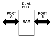
Memory devices and systems are diversifying and becoming more complex out of necessity to support information processing needs. The need to centralize data storage in multiprocessor applications challenges both hardware and software designers. New ways must be found that consolidate system information that is controllable by more than one bus. In addition, systems are becoming more power conscious, particularly portable systems as they typically rely on some kind of rechargeable battery for power. For systems where shared bus access requirements are infrequent, but require many megabytes of memory to be transferred, a shared mass storage device such as a floppy disk drive or networked hard disk drive may suffice. However, for frequent, low density access, media such as hard drives or floppy diskettes are impractical and would greatly slow the rate at which data could be stored and retrieved. The DS1609 Dual Port Ram has been specifically designed to be able to meet high frequency, low volume data storage and retrieval between two asynchronous systems. With its ability to operate at voltages as low as 2.5 volts, the DS1609 also fits easily into any portable application where power availability is limited.
Pin Assignment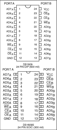
The type of bus which may be connected to either port of the DS1609 is not limited to system level. A multiplexed microprocessor address and data bus can be connected directly to either or both ports of the DS1609. The device can be controlled from either bus port separately by only three signals, "active-low OE", "active-low CE", and "active-low WE". The obvious disadvantage of the multiplexed bus is the slightly reduced system performance because address and data information is being transmitted serially . The equally obvious advantage is the reduced pin count achievable by multiplexing the addressing and data buses.
Read / Write access of either port is transferred as 8 bits address, followed by 8 bits of data. In a read cycle to a port, "active-low WE" is inactive, and the cycle is initiated when "active-low CE" goes active, which with the address latched, data is retrieved under the control of "active-low OE". The rising edge of either "active-low CE" or "active-low OE" terminates the read cycle. For a write cycle , "active-low OE" is inactive, and "active-low CE" becoming active latches the address to be accessed, with "active-low WE" becoming active.
The DS1609 dual port RAM has a special cell design that allows for simultaneous accesses from two ports. Because of this cell design, no arbitration is required for read cycles occurring at the same instant. However, an argument for arbitration can be made for reading and writing the cell at the exact same instant or a write from both ports at the same instant. If a write cycle occurs while a read cycle is in progress, the read cycle will likely recover either the old data or new data and not some combination of both. However, the write cycle will update the memory with correct data. Simultaneous write cycles to the same memory location pose the additional concern that the cell may be in contention causing a metastable state. Depending on the timing of the write cycles of port A and port B, the memory location could be left containing the data written from port A or the data from port B or some combination thereof. However, both concerns expressed above can be eliminated by disciplined system software design. A simple way to assure that read / write contention does not occur is to perform redundant read cycles. Write / write contention needs can be avoided by assigning groups of addresses for write operations to one port only. Groups of data can be assigned check sum bytes which would guarantee correct transmission. A software arbitration system using a "mail box" to pass status information can also be employed. Each port could be assigned a unique byte for writing status information which the other port would read. The status information could tell the reading port if any activity is in progress and indicate when activity is going to occur.
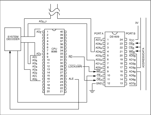
Figure 1. DS1609 dual port interface to Intel 8086 microprocessor.
The DS1609 is ideally suitable for small microprocessor based systems which frequently utilize dedicated 8 bit multiplexed address / data busses the following examples deal with interfacing with the Intel 8086/8088 series and the Motorola HC11 series microprocessors.
For implementation with the Intel 8086/8088 microprocessor family, the address / data pins of either port may be tied directly to the lower 8 address data lines of the Intel 8086 or 8088 microprocessor (Figure 1). The active-low RD pin from the microprocessor provides the "active-low OE" input to the port on the DS1609, while active-low WR provides the "active-low WE" input to the port. The port's "active-low CE" input may be conditioned by a system decoder, which would require the 8086's ALE output as an input to provide address latching. Several of the unused address / data lines from the 8086 would also be required as inputs to indicate where the DS1609 resides in the system memory map. In applications where multiple DS1609 ports are required, multiple "active-low CE" outputs could be provided from a system decoder using the ALE signal from an Intel 8086/8088 with user specified address lines to generate multiple chip selects (Figure 3).
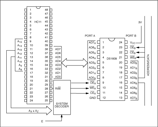
Figure 2. Motorola HC11 expanded mode.
For implementation with the Motorola HC11 microprocessor family, the address / data pins of either port on a DS1609 may be directly ties to port C of an HC11 operating in expanded mode (Figure 2). Address pins from port B of the HC11 (A8- A15) may be used to provide the DS1609's location in the system memory map. The E signal, which is also an input to the HC11, provides a bus clock to the system decoder indicating whether the HC11 is in an address or data cycle. The R / active-low W input to the decoder indicates whether the HC11 is writing or reading data in a data cycle. From these inputs, a system decoder can provide "active-low OE", "active-low WE", and "active -low CE "outputs to DS1609. For applications where more density is required, two DS1609's may be used. The same inputs, including a user selected combination of address lines A8-A15 can be used to provide" active-low OE "," active-low WE ", and multiple" active-low CE "signals for individual DS1609 devices (Figure 4). The DS160 9 may be used with other microprocessors without multiplexed busses, which have a separate address and data bus.
The DS1609 may be used with other microprocessors without multiplexed busses, which have a separate address and data bus.
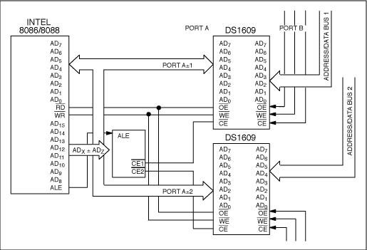
Figure 3. Multiplexed interface.
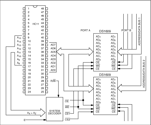
Figure 4. Motorola HC11 expanded mode multiple DS1609's.
The DS1609 can be used as a go between with non-multiplexed microprocessors such as the Intel 386 or Motorola 68030. Processor cycles to and from a DS1609 must then be multiplexed specifically for the DS1609's address / data / bus. An example implementation is shown below (Figure 5).
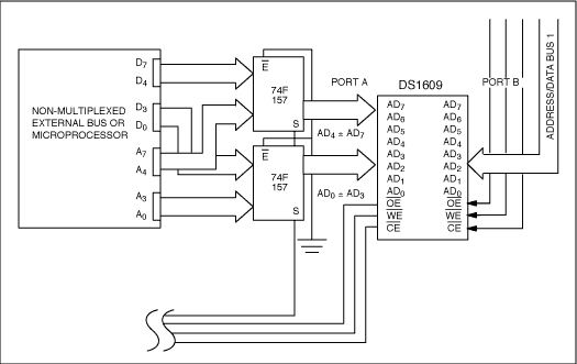
Figure 5. Sample implementation; non-multiplexed bus.
In this implementation, the lower 8 bits of a microprocessor's address bus and data bus are connected to the multiplexed address and data inputs using two 74F157 quad 2 input multiplexers. Each of the 74F157 devices takes 4 address and 4 data inputs originating from a microprocessor or an external bus master. The 74F157s produce four outputs of multiplexed address / data information which can then be used by a DS1609 port. The "active-low E" inputs of each 74F157 may be tied to ground. The S inputs on the 74F157's become control logic, and direct switching back and forth between passing the address lines or the data lines. Read and write enabling signals must be provided by the microprocessor or external bus master.
In SummaryThe DS1609 Dual Port RAM is tailored for use with 8 bit multiplexed address / data bus microprocessors. The DS1609's unique asynchronous dual port access allows a system design to provide a 256 bytewide registers which may be shared by two independent microprocessors. Multiple DS1609's may be tied together in a system to provide for 3 microprocessors having access to two 256 byte memories. Because of the multiplexed address / data bus, pin count and cost are kept to a minimum while providing for the unique asynchronous access. For systems which do not have a multiplexed address / data bus, minimal logic can convert separate address and data lines into a multiplexed address / data bus usable by the DS1609.
Memory devices and systems are diversifying and becoming more complex out of necessity to support information processing needs. The need to centralize data storage in multiprocessor applications challenges both hardware and software designers. New ways must be found that consolidate system information that is controllable by more than one bus. In addition, systems are becoming more power conscious, particularly portable systems as they typically rely on some kind of rechargeable battery for power. For systems where shared bus access requirements are infrequent, but require many megabytes of memory to be transferred, a shared mass storage device such as a floppy disk drive or networked hard disk drive may suffice. However, for frequent, low density access, media such as hard drives or floppy diskettes are impractical and would greatly slow the rate at which data could be stored and retrieved. The DS1609 Dual Port Ram has been specifically designed to be able to meet high frequency, low volume data storage and retrieval between two asynchronous systems. With its ability to operate at voltages as low as 2.5 volts, the DS1609 also fits easily into any portable application where power availability is limited.
Pin Assignment
| Pin | Description |
| VCC | +5 Volt Supply |
| GND | Ground |
| AD0-AD7 | Port Address / Data |
| "active-low CE" | Port Enable |
| "active-low OE" | Output Enable |
| "active-low WE" | Write Enable |
The type of bus which may be connected to either port of the DS1609 is not limited to system level. A multiplexed microprocessor address and data bus can be connected directly to either or both ports of the DS1609. The device can be controlled from either bus port separately by only three signals, "active-low OE", "active-low CE", and "active-low WE". The obvious disadvantage of the multiplexed bus is the slightly reduced system performance because address and data information is being transmitted serially . The equally obvious advantage is the reduced pin count achievable by multiplexing the addressing and data buses.
Read / Write access of either port is transferred as 8 bits address, followed by 8 bits of data. In a read cycle to a port, "active-low WE" is inactive, and the cycle is initiated when "active-low CE" goes active, which with the address latched, data is retrieved under the control of "active-low OE". The rising edge of either "active-low CE" or "active-low OE" terminates the read cycle. For a write cycle , "active-low OE" is inactive, and "active-low CE" becoming active latches the address to be accessed, with "active-low WE" becoming active.
The DS1609 dual port RAM has a special cell design that allows for simultaneous accesses from two ports. Because of this cell design, no arbitration is required for read cycles occurring at the same instant. However, an argument for arbitration can be made for reading and writing the cell at the exact same instant or a write from both ports at the same instant. If a write cycle occurs while a read cycle is in progress, the read cycle will likely recover either the old data or new data and not some combination of both. However, the write cycle will update the memory with correct data. Simultaneous write cycles to the same memory location pose the additional concern that the cell may be in contention causing a metastable state. Depending on the timing of the write cycles of port A and port B, the memory location could be left containing the data written from port A or the data from port B or some combination thereof. However, both concerns expressed above can be eliminated by disciplined system software design. A simple way to assure that read / write contention does not occur is to perform redundant read cycles. Write / write contention needs can be avoided by assigning groups of addresses for write operations to one port only. Groups of data can be assigned check sum bytes which would guarantee correct transmission. A software arbitration system using a "mail box" to pass status information can also be employed. Each port could be assigned a unique byte for writing status information which the other port would read. The status information could tell the reading port if any activity is in progress and indicate when activity is going to occur.
Figure 1. DS1609 dual port interface to Intel 8086 microprocessor.
The DS1609 is ideally suitable for small microprocessor based systems which frequently utilize dedicated 8 bit multiplexed address / data busses the following examples deal with interfacing with the Intel 8086/8088 series and the Motorola HC11 series microprocessors.
For implementation with the Intel 8086/8088 microprocessor family, the address / data pins of either port may be tied directly to the lower 8 address data lines of the Intel 8086 or 8088 microprocessor (Figure 1). The active-low RD pin from the microprocessor provides the "active-low OE" input to the port on the DS1609, while active-low WR provides the "active-low WE" input to the port. The port's "active-low CE" input may be conditioned by a system decoder, which would require the 8086's ALE output as an input to provide address latching. Several of the unused address / data lines from the 8086 would also be required as inputs to indicate where the DS1609 resides in the system memory map. In applications where multiple DS1609 ports are required, multiple "active-low CE" outputs could be provided from a system decoder using the ALE signal from an Intel 8086/8088 with user specified address lines to generate multiple chip selects (Figure 3).
Figure 2. Motorola HC11 expanded mode.
For implementation with the Motorola HC11 microprocessor family, the address / data pins of either port on a DS1609 may be directly ties to port C of an HC11 operating in expanded mode (Figure 2). Address pins from port B of the HC11 (A8- A15) may be used to provide the DS1609's location in the system memory map. The E signal, which is also an input to the HC11, provides a bus clock to the system decoder indicating whether the HC11 is in an address or data cycle. The R / active-low W input to the decoder indicates whether the HC11 is writing or reading data in a data cycle. From these inputs, a system decoder can provide "active-low OE", "active-low WE", and "active -low CE "outputs to DS1609. For applications where more density is required, two DS1609's may be used. The same inputs, including a user selected combination of address lines A8-A15 can be used to provide" active-low OE "," active-low WE ", and multiple" active-low CE "signals for individual DS1609 devices (Figure 4). The DS160 9 may be used with other microprocessors without multiplexed busses, which have a separate address and data bus.
The DS1609 may be used with other microprocessors without multiplexed busses, which have a separate address and data bus.
Figure 3. Multiplexed interface.
Figure 4. Motorola HC11 expanded mode multiple DS1609's.
The DS1609 can be used as a go between with non-multiplexed microprocessors such as the Intel 386 or Motorola 68030. Processor cycles to and from a DS1609 must then be multiplexed specifically for the DS1609's address / data / bus. An example implementation is shown below (Figure 5).
Figure 5. Sample implementation; non-multiplexed bus.
In this implementation, the lower 8 bits of a microprocessor's address bus and data bus are connected to the multiplexed address and data inputs using two 74F157 quad 2 input multiplexers. Each of the 74F157 devices takes 4 address and 4 data inputs originating from a microprocessor or an external bus master. The 74F157s produce four outputs of multiplexed address / data information which can then be used by a DS1609 port. The "active-low E" inputs of each 74F157 may be tied to ground. The S inputs on the 74F157's become control logic, and direct switching back and forth between passing the address lines or the data lines. Read and write enabling signals must be provided by the microprocessor or external bus master.
In SummaryThe DS1609 Dual Port RAM is tailored for use with 8 bit multiplexed address / data bus microprocessors. The DS1609's unique asynchronous dual port access allows a system design to provide a 256 bytewide registers which may be shared by two independent microprocessors. Multiple DS1609's may be tied together in a system to provide for 3 microprocessors having access to two 256 byte memories. Because of the multiplexed address / data bus, pin count and cost are kept to a minimum while providing for the unique asynchronous access. For systems which do not have a multiplexed address / data bus, minimal logic can convert separate address and data lines into a multiplexed address / data bus usable by the DS1609.
Intel is a registered trademark of Intel Corporation.
Motorola is a registered trademark of Motorola, Inc.
Zinc Wire is a good anti-corrosion material,widely used in steel structure anti-corrosion,wind power tower,bridge,sluice gate,oil pipe on sea,Ductile Iron Pipe,extrusion division tube.
|
|
Zinc Wire
Zinc Wire,High Pure Zinc Wire,Zinc Wire Mesh,Corrosion Protection Zinc Wire
Shaoxing Tianlong Tin Materials Co.,Ltd. , https://www.tianlongspray.com