The rapid changes in today's data-acquisition systems are pushing the manufacturers of semiconductor data converters to provide ever-higher levels of resolution, clock speed, and dynamic performance. Because these requirements cannot always be met with a single chip, they demand creativity from the system designer.
Time-interleaving an existing group of high-speed ADCs can multiply the sampling speed of a system, but it becomes a tricky and complex chore at higher sampling speeds. The following discussion lends insight into this technique, covers the positive and negative aspects of such designs, and provides valuable theory on the successful interleaving of multiple ADCs in a high-speed data-acquisition system.
What Is Time Interleaving? For very-high-speed applications, time interleaving increases the overall sampling speed of a system by operating two or more data converters in parallel. This sounds reasonable and straightforward but actually requires much more effort than just paralleling two ADCs. Before discussing this arrangement in detail, compare the sampling rate of a time-interleaved system with that of a single converter. As a rule of thumb, operating N number of ADCs in parallel increases the system's sampling rate by approximately a factor of N. Thus , the sampling (clock) frequency for an interleaved system that hosts N ADCs¹ can be described as follows:
 The simplified block diagram in Figure 1 illustrates a single-channel, time-interleaved DAQ system in which two ADCs double the system's sampling rate. This rate (fSYSTEM_CLK) is a clock signal at twice the rate of fCLK1 = fCLK2. Because fCLK1 is delayed with respect to fCLK2 by the period of fSYSTEM_CLK, the two ADCs sample the analog input signal alternately, producing an overall sample rate equal to fSYSTEM_CLK. Each converter operates at half the sampling frequency.
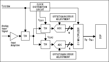
Figure 1. This simplified block diagram depicts a two-step, time-interleaved ADC system for high-speed data acquisition.
How Does Time Interleaving Work? A typical time-interleaved system can be explained by analyzing the operation of an N-bit two-step flash converter. ADCs featuring clock speeds greater than several hundred megahertz often have a multi-step²time-interleaved architecture rather than a single-step direct-conversion (pure flash) architecture (see the appendix for a discussion of flash conversion).
To increase the sampling rate of an ADC whose comparators are already running at maximum speed, the number of upper (coarse) and lower (fine) quantizer blocks must be extended. This can be achieved by implementing an N-bit, coarse ADC and two time-interleaved, N-bit, fine ADCs (Figure 2). The coarse quantizer CQ determines the upper bits (MSBs), and the fine quantizers FQ1 and FQ2 set the lower bits (LSBs) of the digital output.
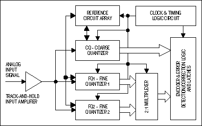
Figure 2. Principle of the time-interleaved two-step flash converter.
The CQ and FQ1 blocks are both connected to the input terminal during the first sampling step, but only the coarse quantizer samples and digitizes at that time. In a second step, information from the coarse quantizer is used by FQ1 and FQ2 to generate the reference levels that enable them to perform a fine quantization. The LSBs are digitized during the time it takes to sample and perform a conversion with the coarse quantizer, and interleaving takes place when sampling the second time.
When the first sampling-and-conversion process has been completed, the input is sampled and digitized by CQ and FQ2. While FQ2 is processing the second sample, CQ is sampling the third time. When the second sample quantization is finished, the third sample is then converted by FQ1. The coarse quantizer is always sampling and converting, but the fine quantizers (FQ1 and FQ2) sample and digitize on alternate cycles. Repeating over and over again, this procedure roughly doubles the overall sampling speed of the two-step ADC system.
What Should Be Considered When Time Interleaving? Pushing the operational limits of interleaved ADCs can be very attractive, but various limitations and considerations must be taken into account before turning this method into a successful experiment.
Bandwidth Limitations: Applications that call for higher sampling speeds usually deal with higher-frequency input tones, so a data converter with an input bandwidth of half the sampling speed would not be suitable for interleaving. Fortunately, most high-speed data converters include track / hold (T / H) amplifiers whose full-power and small-signal bandwidths are significantly higher than that called for by the Nyquist (fSAMPLE / 2) criteria.
Offset and Gain Errors: The channel-to-channel matching of offset and gain in separate ADCs is not trimmed, so gain and offset mismatches between ADCs are parameters of concern in a time-interleaved system. If one ADC shows an offset and the other a gain error, the digitized signal represents not only the original input signal but also an undesired error in the digital domain. An offset discrepancy causes a signal phase shift in the digitized signal, and gain mismatches show up as differences in signal amplitude. For interleaving designs, you should therefore choose ADCs with integrated gain and offset correction or include external circuitry that allows you to correct these mismatches.
Nonlinearities: Integral nonlinearity (INL) is described as the deviation of the actual transfer function from a straight line, either in LSBs or in percent of full-scale range (% FSR). INL errors of ± 1LSB are quite common for individual ADCs, but in an interleaving system such errors can easily double, causing output-code errors that resemble the offset and gain problems discussed above. The appearance of nonlinearity introduces distortion into the system, which degrades dynamic parameters such as signal-to-noise and distortion ratio (SINAD) and effective number of bits (ENOB).
Clock Phase Jitter and Noise: The signal used as a system clock should have the lowest possible phase noise. Introducing a D-type flip-flop in a divide-by-two configuration reduces the otherwise stringent requirement for a precise 50% duty cycle. You should choose a clock circuit commensurate with the signal source's frequency range, amplitude, and slew rate. A low slew rate on the digitized signal relaxes the jitter requirement on the clock. If this slew rate is large, however, the clock jitter must be minimized. For a full-scale-amplitude sinusoidal input signal, the maximum suggested signal-to-noise ratio (SNR) due to clock jitter only is
ApplicationBy evaluating and analyzing the performance of an actual circuit, we can confirm the theoretical approach presented here. The test setup suggested in Figure 3, for instance, is based on the use of two MAX1444 evaluation boards³ from Maxim. The MAX1444 offers the lowest- speed grade (40Msps) available in Maxim's new 10-bit + 3.3V single-supply high-speed data-converter family. Because it is highly unlikely that two off-the-shelf test boards are precisely matched, take care in connecting the signal sources (clock- and analog-input signal generators) to the boards: Analog and clock inputs must be impedance-matched as specified by the evaluation kit. To avoid further mismatch, cables from signal sources to the boards must be of the same length. Termination resistors should be matched closely to avoid reflections. Clock- and analog-input signal source generators must be phase-locked for proper operation.
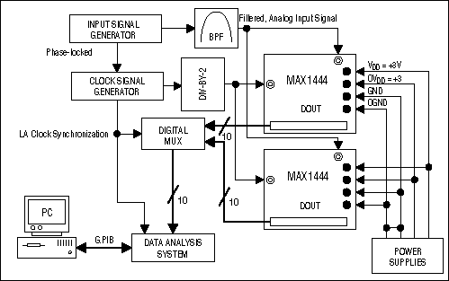
Figure 3. Possible setup to test two MAX1444 evaluation kits for their suitability for use in time-interleaved systems.
Appendix Flash ConversionADCs based on direct-conversion, or flash, architectures are extremely fast and perform their multi-bit conversion directly. Intensive analog design, however, is necessary to manage the large number of comparators and reference voltages required. A pure flash converter with N-bit resolution has 2N-1 comparators connected in parallel. The reference voltages for these comparators are set by a resistor network and spaced 1LSB = VFS / 2N apart, where VFS represents the converter's full-scale input range and N its resolution.
A change of input voltage usually produces a change of state in more than one comparator output. These output changes are combined in an encoder-logic unit (2N-1-to-N encoder) that produces a parallel N-bit output from the converter Although flash converters are the fastest types available, their resolution4 is usually constrained by die size, input capacitance, and power consumption introduced by the large number of internal high-speed comparators. Additionally, the repetitive structure of flash converters demands precise matching between the parallel comparator sections, because any mismatch can cause static error (for example, increased input offset voltage).
Flash ADCs are also prone to sporadic and erratic outputs known as "sparkle codes." Sparkle codes have two major sources: metastability in the 2N-1 comparators and "thermometer-code bubbles." Mismatched comparator delays can turn a logical 1 into 0 ( or vice versa), causing the appearance of "bubbles" in an otherwise normal thermometer code. Because the ADC's encoder unit cannot detect this error, it generates an out-of-sequence code that appears as a "sparkle" output. However, most new data-converter designs minimize or completely eliminate these problems by supporting comparator arrays and encoding logic with additional latches.
_________________________
¹Each ADC operates on the same clock frequency (fCLK1 = fCLK2 = ... = fCLKN) as its adjacent neighbors.
²For simplification and close-comparison purposes, we consider the example of an interleaved two-step architecture.
³ Evaluation boards let you measure channel-to-channel or lot-to-lot mismatches and their effect on the performance of a time-interleaved system.
4 A 1-bit increase in resolution requires doubling the number of comparators.
Literature Sources MAX1444 data sheet, Rev. 0, 8/00, Maxim Integrated Products.
MAX1448EVKIT data sheet, Rev. 0, 0/00, Maxim Integrated Products.
Analog Integrated Circuit Design, D. Johns and K. Martin, John Wiley & Sons Inc., 1997.
Integrated Analog-to-Digital and Digital-to-Analog Converters, R. van de Plasche, Kluwer Academic Publishers, 1994.
Mixed-Signal and DSP Design Techniques, Engineering Staff of Analog Devices Inc., printed by Analog Devices, 2000.
Pipeline ADCs Come of Age A similar version of this article appeared in the February 2001 issue of Sensors magazine.
Security and protection system (SPS) security & protection system, in order to maintain social public safety, the use of security products and other related products constitutes an intrusion alarm system, video security monitoring system, access control system, BSV LCD video wall system, access control fire System, explosion-proof safety inspection system, etc.
Security mainly includes: closed-circuit monitoring system, anti-theft alarm system, building intercom system, parking plant management system, community card system, infrared perimeter alarm system, electronic fence, patrol system, attendance access control system, security room system, electronic examination room system , smart door locks, and more.
As technology continues to advance, the security industry continues to expand. Specialized services such as alarm operation, intermediary, and information began to take off; the product range has been continuously enriched, and it has developed into dozens of categories, such as video surveillance, entrance and exit control, intrusion alarm, explosion-proof security, and thousands of varieties; closed-circuit monitoring is developing rapidly.
Security Pcb,Security System Circuit Board ,Security Pcb Circuit Board,Security Printed Circuit Board
Chuangying Electronics Co.,Ltd , https://www.cwpcb.com