As more and more phones support Bluetooth, Bluetooth headsets have become a must-have option for mobile phones. At the same time, with the introduction of stereo Bluetooth headsets that support MP3 playback, Bluetooth headsets have been able to connect to Bluetooth mobile phones and music players at the same time, which will definitely bring new highlights to Bluetooth applications. This article introduces the design of Bluetooth headset and headphone amplifier.
Bluetooth headset system circuit design
introduction
Bluetooth (Bluetooth Technology) is a short-range wireless communication protocol standard initiated by information technology companies such as Ericsson, Nokia, Motorola, Intel, IBM and Hitachi. Because Bluetooth technology has low power consumption, strong anti-interference ability, suitable for a variety of communication places and relatively simple integrated circuits, Bluetooth technology has broad market prospects as a wireless interface technology to replace wired cables. Bluetooth technology is becoming the standard configuration in mobile phones, PDAs, MP3 players and computers. One of the mainstream applications of Bluetooth technology is to enjoy the high-quality music and hands-free calls sent by the Bluetooth interface of the above products through Bluetooth headsets. In addition to the advancement of technology itself, it is also closely related to the realization of the cost. The price of Bluetooth headsets on the market is as low as a few hundred, and thousands of dollars, while the price of mobile phones itself is mostly less than a thousand dollars. Relatively high price has led to its market penetration speed and breadth is far lower than mobile phones. This article officially based on this XIAN, based on CSR Bluetooth chip BC358239A proposed a low-cost Bluetooth headset circuit design, the popularity of Bluetooth headset will start To an important role.
one. Bluetooth headset architecture and chip introduction
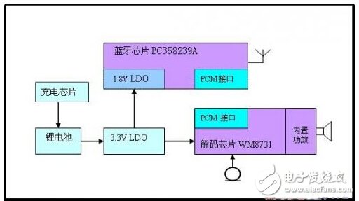
Figure 1 Structure of a Bluetooth headset
In addition to low cost, low power consumption, and simple peripheral circuits, the chip applied to the Bluetooth headset is also very important for providing complete software development tools and small chip package. The following is a brief introduction to the main chips of the Bluetooth headset.
1. BC358239A introduces:
BC358239A chip frequency range 2.402 ~ 2.480Ghz, the transmission power can be up to +4dB, built-in 8-bit DAC (digital-to-analog converter) can automatically adjust the transmit power, no external BALUN (balanced unbalance converter and amplifier can meet Bluetooth V1.2 Specifications; 0.1% BER (bit error rate) typical receiving sensitivity -85dB; fully integrated frequency synthesizer, can support 8 ~ 40Mhz external clock input and external CRISTAL (crystal oscillator); internal integrated DSP (digital signal processor) Speed ​​up to 32MIPS, 32bit instruction word, 24bit data memory, built-in 4K word program memory, two 8K word data memory, enough to support the needs of headphone application software design; on-chip LDO (low dropout linear regulator), support u-law and A-law voice code conversion, support I2S and support PCM voice interface, deep sleep mode power consumption does not exceed 10uA; 10x10mm LFBGA package, only a small PCB size. BC358239A internal structure shown in Figure 2.
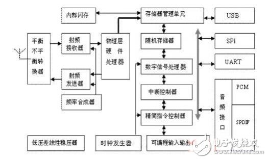
Figure 2 BC358239A internal structure
In addition, BC358239A also has a built-in LDO, its output voltage is 1.8V, and its maximum output current can reach 70mA, which can fully meet the needs of the Bluetooth chip itself.
The Bluetooth software architecture of the BC358239A is quite flexible. Bluetooth applications can run outside of the BC358239A or be handled by an internal RISC processor.
2. Introduction to WM8731
The WM8731 is a CODEC (codec) for voice applications from WOLFSON. It provides a bias voltage for its own MIC (microphone) input. There are two sets of ADCs (analog-to-digital converters) and DACs. Mode converter), the sampling frequency is from 8KHz to 96KHz. The serial control interface can be selected as two-wire and three-wire. Its audio interface can be programmed to be in the form of an I2S or PCM interface. The 28Pin5x5x0.9mm QFN package is ideal for applications where PCB area is limited. The power consumption is extremely low. When the PCM interface is used for communication, the current is free of 20mA. The correct setting of the register can keep the standby power consumption below 15uA.
3. Charging chip SC805 and LDO RT9169-3.3
SEMTECH's SC805 is a powerful CCCV (constant current and constant voltage) charging chip, programmable pre-charge, fast charge and stop charging current, so that it can be combined with PMU (power management) chip into a charge management circuit. It can also be used as a lithium battery charge control chip alone. Thermal protection, overcurrent protection, and battery charging voltage accuracy of 1% make it safe and reliable; input voltage range from 3V to 6V, charging current up to 1A, 3x3mm MLP package, suitable for consumer electronics.
RT9169-3.3 is a 100mA low noise 3.3VLDO produced by RICHTECH. It has a low quiescent current (down to 4uA) and a high ripple rejection ratio. It meets the power requirements of the Bluetooth headset WM8731 and the internal LDO of the Bluetooth chip.
two. Key points in circuit design and software design.
The switch and volume adjustment of the headphone power supply can use the PIO port of the Bluetooth chip BC358239A; when sending the 3.3V power from the RT9169 output to the Bluetooth built-in LDO input, pay attention to the appropriate decoupling capacitor at the input end, VDD_ANA of the Bluetooth chip (built-in LDO1. The 8V output terminal must be added with a decoupling capacitor to prevent the Bluetooth RF offset from being excessively induced by the power supply to the Bluetooth chip. At the same time, the external CrisTIal (crystal oscillator) accuracy of the Bluetooth requires at least 10PPM, otherwise the Bluetooth RF indicator will be affected. .
The WM8731's power input terminals HPVDD, DCVDD, DBVDD, and AVDD can all be used with the LDORT9169's 3.3V output. The proper decoupling at the WM8731's power supply can improve the audio quality of the WM8731 output. The WM8731 clock can utilize the Bluetooth chip's AIO3 pin. Programming clock output. When the WM8731 is connected to the PCM interface of the BC358239A, the ADCLRC and DACLRC of the WM8731 are simultaneously connected to the Bluetooth PCM_SYNC.
BCHS (BluecoreHostSoftware) is a development software provided by CSR to provide customers with Bluetooth product design. BCHS and Bluetooth protocol stack together form a software solution for Bluetooth products. The software architecture of the Bluetooth headset can refer to Figure 4.
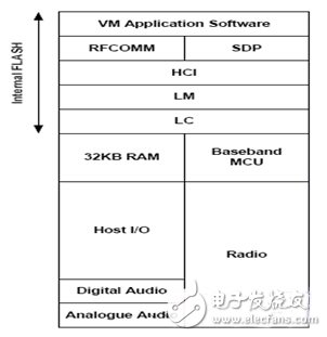
Figure 3 Bluetooth headset software architecture
In Figure 3, VMApplicaTIonsoftware (Virtual Machine Application Software) includes TCS (Telephone Control Protocol), which defines the control signaling for Bluetooth headsets to establish voice and data calls, defines the mobility management process for handling Bluetooth TCS device groups; application functions include The I2C bus writes the WM8731 register to control the headphone volume, battery low voltage alarm and other functions.
in conclusion:
The low-cost solution for Bluetooth headsets is always accompanied by the price reduction of Bluetooth and voice decoding chips. With the rapid spread of Bluetooth interfaces in mobile phones, PDAs, MP3 players and computers, the replacement of wired headsets with Bluetooth headsets has become a technological development. The inevitable trend.
The latest collection of Bluetooth smart technology data, please pay attention to this week's Designs of week - let your smart Bluetooth product design no longer be resigned!
The open frame touchscreen monitor is a product developed and designed by ourselves. It has been sold for more than 6 years and has exceeded 160,000 units. At present, it is running very well. It mainly customizes different touch technologies, different sizes, different interfaces, connecting cables and power supply parts to meet the needs of guests. Our open frame capacitive touchscreen monitor used of PCAP 10 points touch technology, and customize various interfaces for customers, such as: VGA, DVI, HDMI, DP and so on. It is mainly used in banks, hospitals, government units, airports, railway stations, supermarkets, real estate and other places.
Open frame Touchscreen monitor(2C series) Product developed by GreenTouch
Size support: 15inch~ 55inches,
Touch technology: Capacitive Touch Screen technology, supports 10-point touch.
Surface support: explosion-proof IK08, dustproof and waterproof IP65.
Standard VESA: 75mm * 75mm and 100mm * 100mm
Input interface: VGA. DVI.HDMI, DP.Mic.Audio out and other combinations.
Input power: DC12V / 4A or AC80-240V,
Product certificate: support CE, FCC, CB, UL ,HDMI certification optionsS
Pruduct Show:


Open Frame For Capacitive Touch Monitor
Open Frame Capacitive Touch Monitor,PCAP Touch Screen Monitor,IP65 Touch Monitor,Portable Touch Screen Monitor,Projected Capacitive Touch Screen Monitor,Touch Screen Display Monitor
ShenZhen GreenTouch Technology Co.,Ltd , https://www.bbstouch.com