With the advent of the information age, handheld electronic products are emerging (such as PDAs, digital cameras, mobile phones, etc.). These products are mainly powered by batteries. How to design power management circuits in such products to ensure the practicability and economy of the products becomes a key issue in product design. This article discusses the design of two typical battery-powered circuits from the working experience of designing handheld products.
1 Hard switch circuit design example
The hard-switching circuit converts the series voltage of two 7-cell batteries into a voltage of 3.3 V through a DC/DC converter MAX756. The circuit diagram is shown in Figure 1. If the battery is directly powered without the booster circuit, there is a high-to-low drop in the voltage generated at the battery terminal. The series voltage of the two new batteries is above 3 V. As the energy is exhausted, it will drop below 2V, causing the machine to malfunction. The JM2 button is an on/off button. When the JM2 is pressed, a malfunction occurs due to the jitter of the button. The charging and discharging circuit composed of R20, C13, R21, R22, R23, V9 functions to make the charging time and discharging time of the charge and discharge circuit larger than the key shaking time by appropriately selecting the values ​​of R20, C13, and R21. Ground to eliminate the jitter of the keys. The button pulse of the V9 collector output is debounced, and then further filtered and shaped by the U25 (74HC14) three inverters with Schmitt trigger to generate a complete pulse of the waveform. The flip of the U24A (74HC74 D flip-flop) is triggered by this pulse.
In Figure 1:
1 If the 5-pin Q terminal of U24A outputs a high level, the 6-pin Q terminal outputs a low level, and the low level is input to the MAX756 pin-inhibited terminal (active low). At this time, the MAX756 is in the off state, but due to the presence of the pulse rectifier V5 in the DC/DC converter circuit, the battery voltage still reaches the output pin 6 of the DC/DC via V5. Therefore, a transistor V11 must also be added as a switching element in the circuit. When the U24A's 6-pin Q terminal outputs a low level to disable the MAX756, the U24A's 5-pin Q terminal outputs a high level to turn off the transistor V11, thus completely shutting off the battery-to-main circuit power supply VCC. State, the machine is in the off state, and the whole machine current is the minimum when it is turned off, and the measurement does not exceed 5uA.
2 When the button pulse triggers U24A (74HC74 D flip-flop) to flip, U24A's 5-pin Q terminal outputs low level, and 6-pin Q terminal outputs high level, MAX756 is in working state, because output voltage control terminal 2 is high level , so output +3.3 V voltage. At the same time, the U24A's 5-pin Q-terminal output low level causes the transistor V11 to be in the on state, so that the MAX756 output can supply the working power to the main circuit, and the machine is turned on.
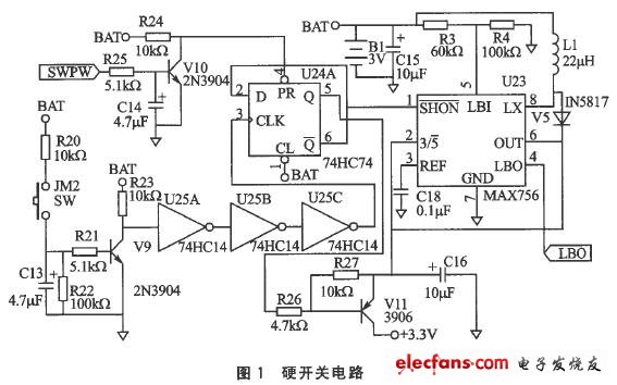
In the power-on state, the output SWPW of the microcontroller is kept low. When the MCU changes the SWPW output to a high level, the inverter circuit formed by V10 outputs a low level, so that U24A is set to 1 terminal, U5A's 5-pin Q terminal outputs a high level, and the 6-pin Q terminal outputs a low level. The machine will be shut down, so SWPW can be used as an "auto power off" signal. Since the 1/O port output is high when the MCU is powered on, the SWPW high level at the reset will cause a “reset false shutdown†phenomenon. In order to prevent this from happening, a charging circuit consisting of R25 and C14 is added to the SWPW output circuit, and the values ​​of R25 and C14 are appropriately selected. After the reset, the voltage is not charged to the V10 conduction threshold at R25 and C14. By setting SWPW low before the level of 0.7 V, the “reset false shutdown†phenomenon can be avoided.
The MAX756's 5-pin LBI is a low-voltage detection pin. If the voltage on this pin drops below the internal reference voltage of 1.25 V, the MAX756's 4-pin LBO (open-drain output) will output a low level. Can be used as a battery low voltage alarm signal. There are two settings for the alarm voltage point.
1 The national standard requires a battery termination voltage of 0.9 V. After actual measurement, when the series voltage of the 2nd 7th battery drops below 2V, the battery energy is about to be exhausted, and the product can not maintain the stable operation. Therefore, set the battery low-voltage detection alarm point to 2 V.
2 The MAX756 alarm voltage U is calculated as:
![]()
The reason why the circuit is called a hard-switching circuit is that the switch can be realized by pressing JM2, and it is not necessary to be assisted by the single-chip microcomputer. The role of SWPW is to achieve a timed automatic shutdown. The battery power supply circuit mentioned next must have a single-chip microcomputer to assist when the button is turned on and off.
2 soft switching circuit design example
In the power management circuit shown in Figure 2, the RN5RK331A DC/DC converter from Ricoh Co., Ltd. is used to convert the voltage supplied by the battery to a voltage of 3.3 V and then supply it to the main circuit to ensure that the machine is in the entire life cycle of the battery. Can work steadily.

The process of turning on/off the circuit is divided into two cases:
1 In the off state, the JM16 button is used as the power button. Press JM16, the battery voltage reaches the base of V5 via V1, which causes V5 and V7 to conduct; the battery voltage passes through V7 to the input and enable terminals of DC/DC converter RN5RK331A, and the DC/DC converter starts to work. The circuit outputs a 3.3 V supply. After the payment cipher enters the power-on state, the P3.6 output low level of the MCU and the V5 and V7 remain in the ON state through the V2 after the reverse phase, so that the payment cipher can maintain the boot even after the JM16 key is released. State, P3.6 output low level to play the role of self-protection.
2 In the power on state, the JM16 button is used as the power off button. When the JM16 button is not pressed, the SWH signal point is low. Press the JM16 button, the SWH signal point is high level. This signal change is read by the MCU through the keyboard interface. When the JM16 is closed at the startup, it can be determined as the shutdown command. When the JM16 button is released, the P3 of the MCU .6 output high level and after inversion, V5 and V7 are turned off by V2, and the payment cipher is turned off because there is no power supply. In the power supply circuit, the transistor V7 is a battery-powered switching element, which is placed in front of the DC/DC converter circuit. When the power is turned off, the power supply circuit of the DC/DC converter is completely cut off, further reducing the leakage current during shutdown. After the whole machine is tested, the shutdown current is less than 5uA. The low-voltage detection alarm of the battery in Fig. 2 is realized by RN5VT20CA (U9) of Ricoh Co., Ltd., and the detection voltage is a fixed value of 2V.
Compared with Figure 1, after booting with JM16 key, it must also use the single-chip P3.6 output low level to realize boot self-protection, so the circuit is called "soft switching circuit". The advantage of using this soft switching circuit is that it does not need to consider the button debounce problem, the hardware circuit is simple, the hardware cost can be reduced, the printed board surface can be saved, and the printed board surface is very valuable in the hand-held product (the number of components) Directly affect the size of the printed board and the overall appearance of the product). The disadvantage is that when the external signal is disturbed or the battery is dead due to insufficient battery power, the button JM16 will not work. The battery must be removed and reloaded to solve the crash. Of course, the probability of this situation is extremely low, and when the battery is dead due to insufficient battery, you need to replace the battery. In the hard-switching circuit of FIG. 1, when a crash occurs, there is no need to touch the battery, and the boot and shutdown can be realized by pressing the button JM2.
3 power supply filtering
In the DC/DC converter circuit described above, a DC/DC boost converter device is used, and the circuit structure of the step-up DC/DC converter is as shown in FIG.
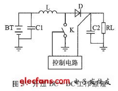
When the switch K is turned on, the battery BT charges the inductor L, and stores energy 1/(2L&TImes; I2) in the form of a field in L. Where I is the inductor current. After K is disconnected, the magnetic energy in L is again released to the filter capacitor C2 and the load RL in the form of electrical energy. The periodic switching operation causes the battery energy to be continuously fed into the load, and the output voltage is converted to:
Vout = Vin/(1-δ)
Where δ is the switching duty cycle (the ratio of the on-time to the duty cycle). The control circuit monitors the output voltage and controls the duty cycle for the purpose of regulating and stabilizing the output voltage. The DC/DC boost converters described in this paper are all controlled by PFM (Pulse Frequency Modulation) and have a small quiescent current. The efficiency is higher under light load conditions, but the ripple is slightly larger. In order to ensure stable operation of the main circuit, it is necessary to consider filtering the power output. Passive filtering circuits are generally used for filtering. The main forms of passive filtering are capacitive filtering, inductive filtering and complex filtering (including inverted L-type, LCπ-type filtering and RCπ-type filtering, etc.). When using inductive filtering or complex inductive filtering, it is necessary to use inductors with high inductance and large volume, which is not suitable for handheld and portable products. Therefore, in the case of small load current, RCπ type filtering is adopted, which is simple and economical. The filtering effect is also better. The equivalent series resistance (ESR) of the filter capacitor is the main factor causing the output ripple. The material of the capacitor should be a ceramic capacitor with a lower ESR, an aluminum electrolytic capacitor and a button electrolytic capacitor. Standard aluminum electrolytic capacitors should be avoided as much as possible. When RCn type filtering is used, the ripple coefficient S = 1 / (Kω & TImes; C & TImes; R) at both ends of the output voltage. K is a constant. It can be seen from this formula that the larger the R is, the larger the C is, the smaller the pulsation coefficient is, that is, the better the filtering effect is. When the value of R increases, the DC voltage drop across the resistor increases, which increases the internal loss of the DC power supply; if the capacitance of C is increased, the volume and weight of the capacitor are increased, which is not easy to achieve. The capacity of the capacitor is generally 10-100 uF, and the value of the resistor is generally less than 10 Ω.
Conclusion
The two battery power supply circuits described above are DC/DC boost circuits that convert the battery voltage to +3.3 V DC voltage to provide working power for the microcontroller application system. This type of circuit is mainly used in PDAs, handheld terminals and other products powered by two 7-cell batteries. The battery power supply circuits of other products (such as mobile phones and digital cameras) will be different, but the working principle is basically similar. In the design of battery-powered circuits, there are a series of problems such as how to implement switching, reduce shutdown current, reduce ripple and interference signals in the output power supply, and improve conversion efficiency. Only by properly solving these problems can we ensure that our products work reliably and reliably. The two examples described in this paper have solved this problem well and have been applied in the product with good results. Of course, as new devices continue to emerge, the design of such circuits needs to be continuously improved and improved to improve the overall performance of the product.
| About Film Covered Wire |
Glass-fiber covered polyester film covered rectangular copper (aluminium) wire .includings Glass-fiber Polyimide Film Covered Flat Copper Wire, Glass-fiber Polyimide Film Covered Flat Aluminium Wire, Glass-fiber Polyester Film Covered flat Copper Wire , Glass-fiber Polyester Film Covered flat Aluminium Wire, Glass-fiber Covered flat Copper wire, Glass-fiber Covered flat Aluminium wire.
Packaging of Products
30/50/150 kg wooden spool
Application: medium and large electrical motor and transformer windings

Film Covered Wire
Aluminium Wire,Film Covered Wire,Polyimide Film Covered Copper Wire,Film Covered Flat Wire
HENAN HUAYANG ELECTRICAL TECHNOLOGY GROUP CO.,LTD , https://www.huaonwire.com