With the rapid development of communication technology and the increasing complexity and transient nature of electrical signals, developers are placing increasing demands on the performance of digital oscilloscopes, an indispensable tool in the measurement field. Maximizing the real-time sampling rate and waveform capture capability has become the focus of many digital oscilloscope manufacturers at home and abroad. The improvement of real-time sampling rate and waveform capture rate will inevitably bring about the transmission, storage and processing of a large number of high-speed waveform data. Therefore, as the backbone of digital oscilloscope data processing and system control, microprocessor performance is critical. This paper selects TI's dual-core DSP OMAP-L138 as the microprocessor of this design, and realizes a digital oscilloscope microprocessor hardware design.
Basic architecture of digital oscilloscope
At present, digital oscilloscopes mostly use DSP, embedded microprocessor type FPGA or microprocessor + FPGA architecture. Although embedded microprocessor-based FPGAs are flexible, they can be fully designed and developed for easy system upgrades and simple FPGA peripheral circuits. However, this type of FPGA is a high-end FPGA, which is expensive and has a rare supply channel. It is not suitable for low-cost digital oscilloscopes. If the DSP is used alone, although its data processing capability is strong and the running speed is high, the control ability of the DSP is not prominent, and the sampling rate of the digital oscilloscope is getting higher and higher, and the DSP cannot internally perform data stream slowdown and buffering. ADCs with high real-time sampling rates require DSPs with higher frequencies and richer internal memory resources. Such DSPs are generally expensive and are not suitable for low-cost digital oscilloscopes. Therefore, the microprocessor + FPGA architecture solution is the first choice for this design. The system structure diagram of the digital oscilloscope with microprocessor + FPGA architecture is shown in Figure 1:
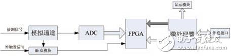
Figure 1 Digital oscilloscope system structure diagram of microprocessor + FPGA architecture
The measured signal is sent to the ADC device through the analog channel op amp; the ADC converter converts the input signal into a corresponding digital signal and buffers and preprocesses it through the FPGA; the microprocessor processes and processes the sampled digital signal. Finally, the waveform is sent to the screen for display to complete an acquisition process. At the same time, the trigger circuit continuously monitors the input signal to see if the trigger state occurs. The trigger condition determines the starting position of the waveform, and the trigger system can ensure that the measured waveform can be stably displayed on the screen.
Microprocessor selection
The real-time sampling rate of this design is as high as 2Gsps, which requires a large amount of waveform data processed by the microprocessor in real time. At the same time, the microprocessor must implement analog channel control, high-speed ADC sampling control, waveform data storage control, and LCD display control. Therefore, a microprocessor with powerful data processing capability and excellent control capability has become the first choice of this design.
Based on these requirements, this design selected TI's OMAP-L138 DSP. This chip is a high-performance processor chip introduced by TI in 2009. The chip features are as follows:
1. It adopts the dual core structure of C6748 DSP core and ARM9 core to achieve unit core frequency up to 300 MHz. With the on-chip ARM9, developers can take advantage of the DSP core to support high-intensity real-time processing and let ARM be responsible for non-real-time tasks.
2. Rich internal memory resources. The ARM core has 16KB L1 program cache and 16KB data cache inside; DSP core adopts L2 cache structure, including 32KB L1 program cache, 32KB data cache and 256KB L2 unified mapping SRAM. The L2 cache structure can be Serving all load, store, and processing requests provides efficient, high-speed data sharing for the CPU. In addition, there is up to 128KB of on-chip RAM between the ARM core and the DSP core, which can be ARM core, DSP core, and off-chip. Memory access.
3. Rich peripheral resources. Mainly includes 1 EMIFA port, can be connected to 16bit SDRAM or NOR/NAND Flash; 1 EMIFB port, can be connected to 16bit DDR2 (highest frequency 150MHz) or 16bit mDDR (highest frequency 133MHz); 3 UART interfaces; 2 SPI interfaces 2 I2C interfaces; 1 EMAC controller; 1 USB2.0 interface and 1 USB1.1 interface; 1 LCD controller; 1 SATA controller; 1 uPP interface; 1 VPIF interface; 64-bit general purpose timer. The rich peripheral resources not only provide an interface for the oscilloscope to communicate with PCs and portable USB interface devices, but also greatly reduce the design scale of DSP peripheral circuits.
4, low power consumption. With a 1.2V core voltage, 1.8V or 3.3VI/O interface voltage, the power consumption is only 6mW in deep sleep mode and 420mW in normal operation mode.
In addition, OMAP-L138 is a floating, fixed-point compatible DSP. It uses hardware to complete floating-point operations and can be completed in a single cycle. This advantage is especially prominent when implementing high-precision complex algorithms, which provides guarantee for real-time processing of complex algorithms. The OMAP-L138 is also pin-to-pin compatible with the C6748 DSP, allowing customers to develop products with many different features simultaneously using different processors.
Hardware structure design of digital oscilloscope system
This design ADC uses AT84AD001 of Atmel Company. The chip has two channels, the sampling rate of each channel is up to 1Gsps, and the real-time sampling rate of 2Gsps can be achieved by flattening. The FPGA selects XC3S400A chip of Xilanx Spartan-3A series, the chip has 8064 Logical units, 360Kbit block RAM, 56Kbit distributed RAM, 4 digital clock management modules (DCM), 311 I/O ports. The 300KB SRAM chip is externally mounted on the FPGA for deep storage. Since the SRAM memory capacity is much larger than the FPGA internal buffer FIFO, it can store more waveform data, so more waveform details can be observed. The 64Mbit SPI Flash storage oscilloscope needs to save data when it is powered down, such as program code, Boot loader program, Chinese and English fonts, boot screen, and so on.
The structure diagram of the oscilloscope hardware system based on OMAP-L138 is shown in Figure 2:

Figure 2 Digital oscilloscope system structure
In this design, the signal to be measured enters the analog channel and is sent to the ADC. After sampling and quantizing the analog signal, the ADC enters the FPGA data stream to slow down and synchronize the data, and then selects to store in the FPGA internal FIFO or save according to the storage depth requirement. Off-chip SRAM, after the internal FIFO of the FPGA or the off-chip SRAM full flag is valid, the DSP reads the sampled data and stores it in the DDR2 SDRAM, and completes a series of complicated processing and operations, such as FFT, interpolation and filtering, and then deposits it in DDR2. The extended display storage area is read by the DSP when the display is needed. The data is sent to the LCD display by the internal integrated LCD controller through the integrated LCD controller to complete the acquisition process.
Interface circuit design of OMAP-L138 and DDR2
The OMAP-L138's integrated DDR2/Mobile DDR controller can be connected to a DDR2 SDRAM operating at 150MHz or a Mobile DDR operating at 133MHz. This design uses DDR2 SDRAM as the system's post-stage waveform data buffer. Compared with SDRAM, DDR2 SDRAM not only greatly increases the read/write speed, but also greatly expands the storage capacity. The oscilloscope can store more waveform data and observe more waveform details, improving the oscilloscope's complex signal and transient signal. Capture probability. The DDR2 SDRAM of this design selects DDR2 800 memory particles of Magnesium Corporation, the model is MT47H64M16, the capacity is 1Gbit, the core working voltage is 1.8V, the core working frequency is 400MHz, because the maximum working frequency of DDR2 controller inside OMAP-L138 is 150MHz, Therefore, DDR2 needs to be down-converted in this system. The interface connection between OMAP-L138 and DDR2 is shown in Figure 3:
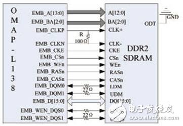
Figure 3 OMAP-L38 and DDR2 interface connection diagram
The signal line of DDR2 includes three parts: clock, data and command. This design provides differential clock CLK+ and CLK- to DDR2 by DDR2 controller. A 100Ω matching resistor is connected between the differential clocks to eliminate the glitch of the clock and limit the driving current. The data part mainly completes the data transmission work, including data. Line DQ[15:0], data synchronization signal DQS (the design LDQS corresponds to the lower eight bits of the data line, UDQS corresponds to the upper eight bits of the data line), and the data signal shielded line DM (masks the data that is not stored during the burst write transfer, The LDM corresponds to the lower eight bits of the data bit DQ[7:0], and the UDM corresponds to the upper eight bits of the data line DQ[15:8]. This design is connected with a 22Ω resistor on the DQS signal and the DM signal to prevent interference and filtering. Function, improve signal quality; the command part includes row address strobe signal RASn, column address strobe signal CASn, write enable signal WEn, chip select signal CSn, clock enable signal CKE, and chip internal termination resistor enable ODT, mainly completed Addressing, composing various control commands and memory initialization work. In this design, since there is no termination resistor in the DDR2 controller, the ODT signal of the DDR2 SDRAM is directly grounded to invalidate the termination resistance in the DDR2 chip.
The read and write timing diagrams of DDR2 are shown in Figure 4 and Figure 5, respectively:

Figure 4 DDR2 read data timing diagram
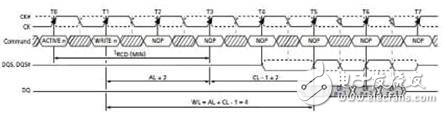
Figure 5 DDR2 write data timing diagram
Ethernet interface circuit design
When measuring electrical signals with an oscilloscope, the convenient storage and sharing of information and measurement results becomes increasingly important. If the digital oscilloscope provides an Ethernet interface, the developer can conveniently share the measurement data and results through the network for remote debugging. The waveform data can also be uploaded to the PC through the network to process and analyze the waveform data on the PC. display.
The OMAP-L138's integrated Ethernet controller (EMAC) supports the IEEE802.3 standard and supports both 10Base-T and 100Base-T Ethernet standards. It is available in both full-duplex and half-duplex modes. Two Ethernet interfaces, MII and RMII.
The LAN8710 Ethernet transceiver is used. The Ethernet transceiver provides two Ethernet interfaces, MII and RMII. This design uses the MII interface to interconnect the LAN8710 and EMAC. The MII interface includes a data interface, a management interface between the MAC and the PHY. The data interface includes two separate channels for the transmitter and receiver, respectively. Each channel has 4 data lines, clocks and control signals, wherein the management interface is a dual signal interface: one is the clock signal and the other is the data signal. The upper layer can monitor and control the PHY through the management interface. The management interface's clock MDC is provided by EMAC up to 8.3MHz; the data signal MDIO is a bidirectional interface that synchronizes with the MDC to control the transceiver and collect status information from the transceiver. The information that can be collected includes link status, transmission speed and selection, power down, low power sleep state, TX/RX mode selection, auto-negotiation control, loopback mode control, and the like.
Figure 6 shows the connection of the Ethernet interface:
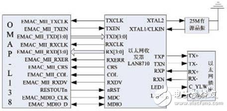
Figure 6 Ethernet interface connection diagram
in conclusion
The design has the following advantages: data processing and system control are synchronously executed; the microprocessor has abundant internal storage resources, adopts a second-level cache structure, and has a fast system response speed; peripheral resources are abundant, and such as USB interface, RS232 interface, and Ethernet are provided. Interfaces such as interfaces and PCs are interconnected to facilitate real-time processing and online debugging of waveform data collected on the oscilloscope; external memory resources are abundant, and 1Gbit capacity DDR2 SDRAM is used as the post-stage waveform data buffer area and display data buffer area. Ability to store more waveform data and observe more waveform details. It can be seen that the oscilloscope system can greatly improve the data processing capability and waveform capture rate of the digital oscilloscope, and the response speed of the whole machine will also reach a higher level.
Led Night Light advantage:
Made with the safety of children in mind, sturdily constructed with toy-grade ABS+PP plastic and provides a 100% safe playing environment,Not too bright, not too dim. Just the right amount of light to see where you are going in the dark.Built-in sensitive light sensor, the nightlight automatically turns on at dusk and off at dawn. 0.5W. 12hrs Each day, only use 2.2 Kwh per year. Never need to replace the bulb.Energy-efficient and eye-caring LED creates a uniform non-flickering light that doesn't hurt the eyes.
Led Night Light,Night Light,Pvc Led Night Light,Kids Led Night Light
Dongguan City Leya Electronic Technology Co. Ltd , https://www.dgleya.com